


 The Marketing Minute: Marketing With Layers
 The Right Approach: Electro-Tek—A Williams Family Legacy, Part 1
 It’s Only Common Sense: If You’re Not Differentiated, You’re Dead


New Ultrathin Capacitor Could Enable Energy-Efficient Microchips
July 18, 2022 | Berkeley LabEstimated reading time: 4 minutes
The silicon-based computer chips that power our modern devices require vast amounts of energy to operate. Despite ever-improving computing efficiency, information technology is projected to consume around 25% of all primary energy produced by 2030. Researchers in the microelectronics and materials sciences communities are seeking ways to sustainably manage the global need for computing power.
The holy grail for reducing this digital demand is to develop microelectronics that operate at much lower voltages, which would require less energy and is a primary goal of efforts to move beyond today’s state-of-the-art CMOS (complementary metal-oxide semiconductor) devices.
Non-silicon materials with enticing properties for memory and logic devices exist; but their common bulk form still requires large voltages to manipulate, making them incompatible with modern electronics. Designing thin-film alternatives that not only perform well at low operating voltages but can also be packed into microelectronic devices remains a challenge.
Now, a team of researchers at Lawrence Berkeley National Laboratory (Berkeley Lab) and UC Berkeley have identified one energy-efficient route – by synthesizing a thin-layer version of a well-known material whose properties are exactly what’s needed for next-generation devices.
First discovered more than 80 years ago, barium titanate (BaTiO3) found use in various capacitors for electronic circuits, ultrasonic generators, transducers, and even sonar.
Crystals of the material respond quickly to a small electric field, flip-flopping the orientation of the charged atoms that make up the material in a reversible but permanent manner even if the applied field is removed. This provides a way to switch between the proverbial “0” and “1” states in logic and memory storage devices – but still requires voltages larger than 1,000 millivolts (mV) for doing so.
Seeking to harness these properties for use in microchips, the Berkeley Lab-led team developed a pathway for creating films of BaTiO3 just 25 nanometers thin – less than a thousandth of a human hair’s width – whose orientation of charged atoms, or polarization, switches as quickly and efficiently as in the bulk version.
“We’ve known about BaTiO3 for the better part of a century and we’ve known how to make thin films of this material for over 40 years. But until now, nobody could make a film that could get close to the structure or performance that could be achieved in bulk,” said Lane Martin, a faculty scientist in the Materials Sciences Division (MSD) at Berkeley Lab and professor of materials science and engineering at UC Berkeley who led the work.
Historically, synthesis attempts have resulted in films that contain higher concentrations of “defects” – points where the structure differs from an idealized version of the material – as compared to bulk versions. Such a high concentration of defects negatively impacts the performance of thin films. Martin and colleagues developed an approach to growing the films that limits those defects. The findings were published in the journal Nature Materials.
To understand what it takes to produce the best, low-defect BaTiO3 thin films, the researchers turned to a process called pulsed-laser deposition. Firing a powerful beam of an ultraviolet laser light onto a ceramic target of BaTiO3 causes the material to transform into a plasma, which then transmits atoms from the target onto a surface to grow the film. “It’s a versatile tool where we can tweak a lot of knobs in the film’s growth and see which are most important for controlling the properties,” said Martin.
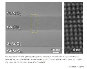
Martin and his colleagues showed that their method could achieve precise control over the deposited film’s structure, chemistry, thickness, and interfaces with metal electrodes. By chopping each deposited sample in half and looking at its structure atom by atom using tools at the National Center for Electron Microscopy at Berkeley Lab’s Molecular Foundry, the researchers revealed a version that precisely mimicked an extremely thin slice of the bulk.
“It’s fun to think that we can take these classic materials that we thought we knew everything about, and flip them on their head with new approaches to making and characterizing them,” said Martin.
Finally, by placing a film of BaTiO3 in between two metal layers, Martin and his team created tiny capacitors – the electronic components that rapidly store and release energy in a circuit. Applying voltages of 100 mV or less and measuring the current that emerges showed that the film’s polarization switched within two billionths of a second and could potentially be faster – competitive with what it takes for today’s computers to access memory or perform calculations.
The work follows the bigger goal of creating materials with small switching voltages, and examining how interfaces with the metal components necessary for devices impact such materials. “This is a good early victory in our pursuit of low-power electronics that go beyond what is possible with silicon-based electronics today,” said Martin.
“Unlike our new devices, the capacitors used in chips today don’t hold their data unless you keep applying a voltage,” said Martin. And current technologies generally work at 500 to 600 mV, while a thin film version could work at 50 to 100 mV or less. Together, these measurements demonstrate a successful optimization of voltage and polarization robustness – which tend to be a trade-off, especially in thin materials.
Next, the team plans to shrink the material down even thinner to make it compatible with real devices in computers and study how it behaves at those tiny dimensions. At the same time, they will work with collaborators at companies such as Intel Corp. to test the feasibility in first-generation electronic devices. “If you could make each logic operation in a computer a million times more efficient, think how much energy you save. That’s why we’re doing this,” said Martin.
This research was supported by the U.S. Department of Energy (DOE) Office of Science. The Molecular Foundry is a DOE Office of Science user facility at Berkeley Lab.
Share on:


Testimonial
"We’re proud to call I-Connect007 a trusted partner. Their innovative approach and industry insight made our podcast collaboration a success by connecting us with the right audience and delivering real results."
Julia McCaffrey - NCAB GroupSuggested Items
ITW EAE Despatch Ovens Now Support ASTM 5423 Testing
10/15/2025 | ITW EAEAs the demand for high-performance electrical insulation materials continues to grow—driven by the rapid expansion of electric vehicles (EVs) and energy storage systems—thermal processing has become a critical step in material development.
Beyond Thermal Conductivity: Exploring Polymer-based TIM Strategies for High-power-density Electronics
10/13/2025 | Padmanabha Shakthivelu and Nico Bruijnis, MacDermid Alpha Electronics SolutionsAs power density and thermal loads continue to increase, effective thermal management becomes increasingly important. Rapid and efficient heat transfer from power semiconductor chip packages is essential for achieving optimal performance and ensuring long-term reliability of temperature-sensitive components. This is particularly crucial in power systems that support advanced applications such as green energy generation, electric vehicles, aerospace, and defense, along with high-speed computing for data centers and artificial intelligence (AI).
Is Glass Finally Coming of Age?
10/13/2025 | Nolan Johnson, I-Connect007Substrates, by definition, form the base of all electronic devices. Whether discussing silicon wafers for semiconductors, glass-and-epoxy materials in printed circuits, or the base of choice for interposers, all these materials function as substrates. While other substrates have come and gone, silicon and FR-4 have remained the de facto standards for the industry.
Creative Materials to Showcase Innovative Functional Inks for Medical Devices at COMPAMED 2025
10/09/2025 | Creative Materials, Inc.Creative Materials, a leading manufacturer of high-performance functional inks and coatings, is pleased to announce its participation in COMPAMED 2025, taking place November 17–20 in Düsseldorf, Germany.
Jiva Leading the Charge Toward Sustainable Innovation
09/30/2025 | Marcy LaRont, PCB007 MagazineEnvironmental sustainability in business—product circularity—is a high priority these days. “Circularity,” the term meant to replace “recycling,” in its simplest definition, describes a full circle life for electronic products and all their elements. The result is re-use or a near-complete reintroduction of the base materials back into the supply chain, leaving very little left for waste. For what cannot be reused productively, the ultimate hope is to have better, less harmful means of disposal and/or materials that can seamlessly and harmlessly decompose and integrate back into the natural environment. That is where Jiva and Soluboard come in.