


 Flexible Thinking: Designing Flex Circuits for Dynamic Reliability
 Global PCB Connections: Rigid-flex and Flexible PCBs—The Backbone of Modern Electronics
 Happy’s Tech Talk #29: Bend-to-Install Semi-flex FR-4


With the rise of Internet of Things and Industry 4.0, piezoelectrics, or materials that generate electric charge when a strain is applied to them, are becoming extremely useful as compact and energy-efficient force sensors. Accordingly, piezotronics has emerged as a new technological frontier with applications in structural health monitoring in civil engineering and human-machine interface devices.
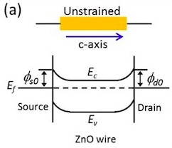
Working mechanism for piezotronic devices with two ends fixed with electrodes on a flexible substrate. This asymmetric tuning of the Schottky barrier height is the piezotronic effect.
Piezotronic force sensors are typically governed by either a strain-induced "Schottky barrier height (SBH) modulation" or by a "piezo-gating effect" that redistributes the charge carriers in an induced piezoelectric field. However, while SBH-based devices have been well-explored, piezo-gating based devices remain relatively less understood. This has limited the fabrication of piezo-gated transistors, the basic building block of all electronics. Additionally, the piezo-gating effect is often confused with the "piezoresistive effect" a co-existing phenomenon with similar response. To harness the full potential of the piezo-gating effect, we, therefore, need to understand it better.
In a new study published in Nano Energy, researchers from National Cheng Kung University (NCKU), Taiwan now report, for the first time, a "dual-mode" piezo-gated thin-film transistor (PGTFT) along with an analytical model explaining its working mechanism. The PGTFT exhibits an unprecedented operation between two modes, namely depletion and accumulation, and a record gauge factor (ratio of relative change in current to mechanical strain) of 2780, indicating its extreme sensitivity.
"PGTFTs relying solely on the piezo-gating effect are essential for developing advanced piezotronic devices. But, most PGTFTs reported so far show indistinct piezo-gating effect through SBH modulation induced by piezoelectric fields, and can detect only one-dimensional strain," says Prof. Chuan-Pu Liu, the corresponding author of the study.
In their work, the researchers used zinc oxide (ZnO) to fabricate the thin-film transistors owing to the versatile piezoelectric and semiconductor properties of ZnO. The charge carrier concentrations in the ZnO thin films were varied in a controlled manner by changing the gas used during their preparation. The thin films were then fully characterized and used to prepare two distinct PGTFT configurations.
The team tested the current-voltage characteristics of the PGTFTs by subjecting them to strain and analyzed the results both analytically and using numerical simulations. Additionally, they explored the effect of changing carrier concentrations on the operation modes of the PGTFTs to gauge the influence of the piezo-gating effect.
The team found that increased strains reduced the current in the top PGTFT electrode but increased it in the bottom electrode. This happened due to the electrons moving from the top to the bottom in response to the force, creating a depletion at the top and an accumulation of electrons at the bottom. This, in turn, affected the output current and revealed the co-existence of piezo-gating effect and piezoresistive effect, with the piezo-gating effect being dominant.
Additionally, the team showed, both experimentally and analytically, that the gauge factor is highly sensitive to the carrier concentration, showing a 44% enhancement in their design.
"Our proposed analytical model explains the workings of the PGTFT perfectly, showing agreement with experiment as well as simulations. These findings will pave the way for the development and application of multi-dimension strain-sensing PGTFTs," says Prof. Liu. This could lead to novel human-machine interfaces that are compact, cost-effective, and less power-hungry.
We may be nearing a piezotronics revolution!


