


 The Government Circuit: From Tax Policy to Tariffs, Denver to Delhi, Speaking Up for Electronics
  Global Sourcing Spotlight: Evaluating a Supplier’s Capabilities
 Global Citizenship: Cultivating Cross-border Partnerships With Integrity


NASA Awards Next-Generation Spaceflight Computing Processor Contract
August 16, 2022 | NASAEstimated reading time: 3 minutes
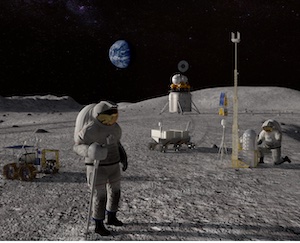
NASA’s Jet Propulsion Laboratory in Southern California has selected Microchip Technology Inc. of Chandler, Arizona, to develop a High-Performance Spaceflight Computing (HPSC)?processor that will provide at least 100 times the computational capacity of current spaceflight computers. This key capability would advance all types of future space missions, from planetary exploration to lunar and Mars surface missions.
“This cutting-edge spaceflight processor will have a tremendous impact on our future space missions and even technologies here on Earth,” said Niki Werkheiser, director of technology maturation within the Space Technology Mission Directorate at NASA Headquarters in Washington. “This effort will amplify existing spacecraft capabilities and enable new ones and could ultimately be used by virtually every future space mission, all benefiting from more capable flight computing.”
Microchip will architect, design, and deliver the HPSC processor over three years, with the goal of employing the processor on future lunar and planetary exploration missions. Microchip’s processor architecture will significantly improve the overall computing efficiency for these missions by enabling computing power to be scalable, based on mission needs. The design also will be more reliable and have a higher fault tolerance. The processor will enable spacecraft computers to perform calculations up to 100 times faster than today’s state-of-the-art space computers. As part of NASA's ongoing commercial partnership efforts, the work will take place under a $50 million firm-fixed-price contract, with Microchip contributing significant research and development costs to complete the project.
"We are pleased that NASA selected Microchip as its partner to develop the next-generation space-qualified compute processor platform.” said Babak Samimi, corporate vice president for Microchip’s Communications business unit. “We are making a joint investment with NASA on a new trusted and transformative compute platform. It will deliver comprehensive Ethernet networking, advanced artificial intelligence/machine learning processing and connectivity support while offering unprecedented performance gain, fault-tolerance, and security architecture at low power consumption. We will foster an industry wide ecosystem of single board computer partners anchored on the HPSC processor and Microchip’s complementary space-qualified total system solutions to benefit a new generation of mission-critical edge compute designs optimized for size, weight, and power.”
Current space-qualified computing technology is designed to address the most computationally-intensive part of a mission – a practice that leads to overdesigning and inefficient use of computing power. For example, a Mars surface mission demands high-speed data movement and intense calculation during the planetary landing sequence. However, routine mobility and science operations require fewer calculations and tasks per second. Microchip’s new processor architecture offers the flexibility for the processing power to ebb and flow depending on current operational requirements. Certain processing functions can also be turned off when not in use, reducing power consumption. This capability will save a large amount of energy and improve overall computing efficiency for space missions.?
“Our current spaceflight computers were developed almost 30 years ago,” said Wesley Powell, NASA’s principal technologist for advanced avionics. “While they have served past missions well, future NASA missions demand significantly increased onboard computing capabilities and reliability. The new computing processor will provide the advances required in performance, fault tolerance, and flexibility to meet these future mission needs.”
Microchip’s HPSC processor may be useful to other government agencies and applicable to other types of future space mission to explore our solar system and beyond, from Earth science operations to Mars exploration and human lunar missions. The processor could potentially be used for commercial systems on Earth that require similar mission critical edge computing needs as space missions and are able to safely continue operations if one component of the system fails. These potential applications include industrial automation, edge computing, time-sensitive ethernet data transmission, artificial intelligence, and even Internet of Things gateways, which bridge various communication technologies.
In 2021, NASA solicited proposals for a trade study for an advanced radiation-hardened computing chip with the intention of selecting one vendor for development. This contract is part of NASA’s High-Performance Space Computing project. HPSC is led by the agency’s Space Technology Mission Directorate’s Game Changing Development program with support from the Science Mission Directorate. The project is led by JPL, a division of Caltech.
Share on:


Suggested Items
OKI, NTT Innovative Devices Establish Mass Production Technology for High-Power Terahertz Devices by Heterogeneous Material Bonding
06/21/2025 | BUSINESS WIREOKI, in collaboration with NTT Innovative Devices Corporation, has established mass production technology for high-power terahertz devices using crystal film bonding (CFB) technology for heterogeneous material bonding to bond indium phosphide (InP)-based uni-traveling carrier photodiodes (UTC-PD) onto silicon carbide (SiC) with excellent heat dissipation characteristics for improved bonding yields.
The Evolution of Picosecond Laser Drilling
06/19/2025 | Marcy LaRont, PCB007 MagazineIs it hard to imagine a single laser pulse reduced not only from nanoseconds to picoseconds in its pulse duration, but even to femtoseconds? Well, buckle up because it seems we are there. In this interview, Dr. Stefan Rung, technical director of laser machines at Schmoll Maschinen GmbH, traces the technology trajectory of the laser drill from the CO2 laser to cutting-edge picosecond and hybrid laser drilling systems, highlighting the benefits and limitations of each method, and demonstrating how laser innovations are shaping the future of PCB fabrication.
Day 2: More Cutting-edge Insights at the EIPC Summer Conference
06/18/2025 | Pete Starkey, I-Connect007The European Institute for the PCB Community (EIPC) summer conference took place this year in Edinburgh, Scotland, June 3-4. This is the third of three articles on the conference. The other two cover Day 1’s sessions and the opening keynote speech. Below is a recap of the second day’s sessions.
Hon Hai Research Institute Achieves Breakthrough in Quantum Cryptography Recognized by Leading Global Conference
06/17/2025 | FoxconnHon Hai Research Institute (HHRI), the research arm of Hon Hai Technology Group (Foxconn), the world’s largest electronics manufacturer and technology service provider, has achieved a significant breakthrough in quantum computing.
Global PCB Connections: Embedded Components—The Future of High-performance PCB Design
06/19/2025 | Jerome Larez -- Column: Global PCB ConnectionsA promising advancement in this space is the integration of embedded components directly within the PCB substrate. Embedded components—such as resistors, capacitors, and even semiconductors—can be placed within the internal layers of the PCB rather than mounted on the surface. This enables designers to maximize available real estate and improve performance, reliability, and manufacturability.