


 Trouble in Your Tank: Understanding Interconnect Defects, Part 1
 It’s Only Common Sense: Marketing Isn’t Fluff, It’s Ammunition
 Driving Innovation: Mechanical and Optical Processes During Rigid-flex Production


Ultrafast Electron Dynamics in Quantum Materials
August 25, 2022 | CAUEstimated reading time: 3 minutes
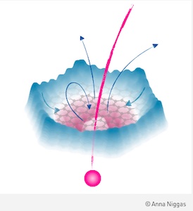
When materials are bombarded with ions, as in the production of tiny structures on semiconductors, highly complex processes take place. A research team from Vienna University of Technology (TU) and Kiel University (CAU) has now been able to reconstruct the extremely fast processes for the first time. To do so, they combined sophisticated measurements with computer simulations. Thus, on a time scale of one femtosecond - the billionth part of a millionth of a second - they showed what happens when an ion penetrates ultra-thin quantum materials such as graphene and molybdenum disulphide. Electrons are emitted from the material in the process, and by comparing them with precise computer simulations, conclusions about details of the processes can be drawn. The results have been published in the current issue of the journal Physical Review Letters and highlighted as Editors’ suggestion.
Highly charged ions swirl up electrons
Prof. Richard Wilhelm's research group at the Institute of Applied Physics at TU Wien works with highly charged ions. Xenon atoms, which have 54 electrons in their neutral state, are stripped of 20 to 40 electrons, and the strongly positively charged xenon ions that remain are then directed onto a thin layer of material.
"We are particularly interested in the interaction of these ions with the material graphene, which consists of only a single layer of carbon atoms," says Anna Niggas from TU Wien, first author of the current paper. "This is because we already knew from previous experiments that graphene has very interesting properties. Electron transport in graphene is extremely fast. During such processes, a large number of electrons are usually also emitted, and we were able to measure their number and energy precisely."
Like molybdenum disulphide, graphene is one of the quantum materials that have also been intensively studied in Kiel for many years. They are characterised by unusual properties based on quantum physical effects. Since both materials are extremely thin, their properties change very drastically when a highly charged ion penetrates them.
Femtosecond travel through quantum materials
Computer simulations should help to understand these experiments. They were developed by Dr. Niclas Schlünzen, in collaboration with Dr. Karsten Balzer, in the research group of CAU-Professor Michael Bonitz at the Institute for Theoretical Physics and Astrophysics. By comparing experiment and theory, the research team was able to jointly unravel what happens during the interaction of the ion with graphene and molybdenum disulphide lasting only a few femtoseconds:
Due to its positive charge, the ion generates an electric field. As soon as it approaches the thin quantum materials, it influences the electrons inside. They move in the direction of the future impact site already before the ion hits. At some point, the electric field of the ion becomes so strong that electrons are torn out of the material and captured by the highly charged ion. Eventually, the ion penetrates the material and a complex interaction occurs: in an extremely short time, the ion transfers a lot of energy to the material, releasing even more electrons into the vacuum. Where electrons are missing in the material, positive charge remains. To compensate for this, electrons quickly move in from other areas of the material.
Computer simulation explains different behaviour of the materials
The precise analysis of these electron movements shows: In graphene, these processes is extremely quickly and strong electron currents form on an atomic scale for a short time. In molybdenum disulphide, on the other hand, the processes take much longer.
The simulations of the researchers from CAU can explain this: they show that the distribution of electrons in the materials in turn strongly influences the electrons that were already released before. The energy distribution of these extracted electrons is very different in the two materials - this allows to draw important conclusions about their properties and the processes taking place inside. Bonitz sums up: "The ion bombardment and the precise experimental and theoretical investigation of the emitted electrons thus represent an important new diagnostic for modern quantum materials that enables an unusually high spatial, temporal and energy resolution."
Share on:


Testimonial
"Advertising in PCB007 Magazine has been a great way to showcase our bare board testers to the right audience. The I-Connect007 team makes the process smooth and professional. We’re proud to be featured in such a trusted publication."
Klaus Koziol - atgSuggested Items
SEMI Foundation Honors Applied Materials at SEMICON West with 2025 Excellence in Achievement Award for Talent Development
11/04/2025 | SEMIThe SEMI Foundation announced it recognized Applied Materials, Inc. with the Excellence in Achievement Award at SEMICON West 2025 in Phoenix, Arizona, honoring the company’s outstanding leadership and collaboration in building the next generation of semiconductor talent.
Sealed for Survival: Potting Electronics for the Toughest Environments
10/29/2025 | Beth Massey, MacDermid Alpha Electronics SolutionsElectronics deployed in harsh conditions face relentless threats from vibration, impact, chemical contaminants, airborne pollutants, and moisture, conditions that can quickly lead to failure without robust protection. Potting, the process of encapsulating electronics in a protective polymer, is a widely used strategy to safeguard devices from both environmental and mechanical hazards.
Driving Innovation: Mechanical and Optical Processes During Rigid-flex Production
10/28/2025 | Kurt Palmer -- Column: Driving InnovationRigid-flex printed circuit boards are a highly effective solution for placing complex circuitry in tight, three-dimensional spaces. They are now indispensable across a range of industries, from medical devices and aerospace to advanced consumer electronics, helping designers make the most efficient use of available space. However, their unique construction—combining rigid and flexible materials—presents a fundamental challenge for PCB manufacturers.
SMTAI 2025 Review: Reflecting on a Pragmatic and Forward-looking Industry
10/27/2025 | Marcy LaRont, I-Connect007Leaving the show floor on the final afternoon of SMTA International last week in Rosemont, Illinois, it was clear that the show remains a grounded, technically driven event that delivers a solid program, good networking, and an easy space to commune with industry colleagues and meet with customers.
ITW EAE Despatch Ovens Now Support ASTM 5423 Testing
10/15/2025 | ITW EAEAs the demand for high-performance electrical insulation materials continues to grow—driven by the rapid expansion of electric vehicles (EVs) and energy storage systems—thermal processing has become a critical step in material development.