


 It’s Only Common Sense: Stay Curious, My Friends
 The Marketing Minute: AI Is Watching Your Marketing Habits


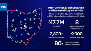
President Joe Biden joins Intel, Ohio Gov. Mike DeWine and other federal, state and local officials to celebrate breaking ground in the Silicon Heartland on two of the world's most advanced chipmaking facilities. As part of Intel’s commitment to develop a skilled talent pipeline for its two new leading-edge chip fabs, Intel also announced the first phase of funding for its Ohio Semiconductor Education and Research Program. During this first phase, Intel is providing $17.7 million for eight proposals from leading institutions and collaborators in Ohio to develop semiconductor-focused education and workforce programs.
“Today marks a pivotal moment in the journey to build a more geographically balanced and resilient semiconductor supply chain. The establishment of the Silicon Heartland is testament to the power of government incentives to unlock private investment, create thousands of high-paying jobs, and benefit U.S. economic and national security. We would not be here today without the support of leaders in the administration, Congress and the state of Ohio, who share a vision to help restore the United States to its rightful place as a leader in advanced chipmaking,” said Pat Gelsinger, Intel CEO.
Semiconductors are the brains behind the technology that powers our digital age. These chips are critical to the foundations of the U.S. economy, national security and technology leadership. Investing to revitalize the U.S. chipmaking ecosystem will bring a broad range of economic benefits, while helping to restore balance, dependability and resilience to the global semiconductor supply chain.
In Ohio, Intel’s more than $20 billion planned investment in a new semiconductor manufacturing site to produce leading-edge chips is expected to generate 7,000 construction jobs and 3,000 long-term positions in manufacturing and engineering. In addition to providing capacity for Intel’s next-generation products, the company expects these new factories to support growing demand for the company’s new foundry business, Intel Foundry Services (IFS).
How Intel Supports U.S. Research and Development (R&D) and Manufacturing: Intel’s investment in Ohio builds on the company’s announcement in Arizona to build two new fabs and its expansion in New Mexico to add advanced packaging capabilities. When combined with Intel’s silicon R&D capabilities, this new site in Licking County, Ohio, will expand the company’s U.S. “lab-to-fab” pipeline.
Intel also recently celebrated the grand opening of the latest expansion of its leading-edge developmental factory in Oregon, where engineers advance Moore’s Law by creating new transistor architectures, wafer processes and packaging technologies that underpin the company’s product roadmap. That investment represents the next phase of Intel’s commitment to driving U.S. leadership in semiconductor research and development.


