


 The Marketing Minute: Marketing With Layers
 The Right Approach: Electro-Tek—A Williams Family Legacy, Part 1
 It’s Only Common Sense: If You’re Not Differentiated, You’re Dead


Siemens Automates 2.5D, 3D IC Design-for-test with New Tessent Multi Die Solution
September 26, 2022 | SiemensEstimated reading time: 2 minutes
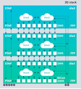
Siemens Digital Industries Software introduced the Tessent Multi-die software solution, which helps customers dramatically speed and simplify critical design-for-test (DFT) tasks for next-generation integrated circuits (ICs) based on 2.5D and 3D architectures.
As demand for smaller, more power efficient and higher performing ICs continues to challenge the global IC design community, next-generation devices increasingly feature complex 2.5D and 3D architectures that connect dies vertically (3D IC) or side-by-side (2.5D) so that they behave as a single device. However, these approaches can present significant challenges for IC test, since most legacy IC test approaches are based on conventional two-dimensional processes.
To address these challenges, Siemens today introduces Tessent Multi-die software -- the industry’s most comprehensive DFT automation solution for highly complex DFT tasks associated with 2.5D and 3D IC designs. The new solution works seamlessly with Siemens’ Tessent™ TestKompress™ Streaming Scan Network software and Tessent™ IJTAG software, which optimize DFT test resources for each block without concern for impacts to the rest of the design, thereby streamlining DFT planning and implementation for the 2.5D and 3D IC era. Using Tessent Multi-die software, IC design teams can rapidly generate IEEE 1838 compliant hardware featuring 2.5D and 3D IC architectures.
“IC design organizations are seeing dramatic spikes in IC test complexity due to the rapid adoption and deployment of designs featuring densely packed dies in 2.5D and 3D devices,” said Ankur Gupta, vice president and general manager of the Tessent business unit for Siemens Digital Industries Software. “With Siemens’ new Tessent Multi-die solution, our customers can be ready for the designs of tomorrow, while slashing test implementation effort and simultaneously optimizing manufacturing test cost today.”
In addition to supporting comprehensive test for 2.5D and 3D IC designs, the Tessent Multi-die solution can generate die-to-die interconnect patterns and enable package level test using the Boundary Scan Description Language (BSDL). Further, Tessent Multi-die supports integration of flexible parallel port (FPP) technology by leveraging the packetized data delivery capabilities of Siemens’ Tessent TestKompress Streaming Scan Network software. Introduced two years ago, Tessent TestKompress Streaming Scan Network decouples core-level DFT requirements from the chip-level test delivery resources. This enables a no-compromise, bottom-up DFT flow that can dramatically simplify DFT planning and implementation, while reducing test time up to 4X.
“As the limits of traditional 2D IC design approaches become increasingly clear over time, more design teams are leveraging the power, performance and form factor advantages that 2.5D and 3D IC architectures can deliver. But deploying these advanced schemes in new design starts without first establishing a DFT strategy that acknowledges the inherent challenges these architectures present can raise costs and undermine aggressive timelines,” said Laurie Balch, president and research director for Pedestal Research. “However, by evolving DFT technology to keep pace with the rapid adoption of multi-dimensional designs, EDA vendors can play a key role in further enabling global, mainstream adoption of 2.5D and 3D architectures.”
Share on:


Testimonial
"In a year when every marketing dollar mattered, I chose to keep I-Connect007 in our 2025 plan. Their commitment to high-quality, insightful content aligns with Koh Young’s values and helps readers navigate a changing industry. "
Brent Fischthal - Koh YoungSuggested Items
Keysight Completes Acquisition of Synopsys’ Optical Solutions Group and Ansys’ PowerArtist
10/17/2025 | Keysight Technologies, Inc.Keysight Technologies, Inc., announced the completion of its acquisitions of the Optical Solutions Group from Synopsys, Inc., and PowerArtist from Ansys, Inc.
RT-Labs Joins STMicroelectronics Partner Program to Accelerate Industrial Communication
10/16/2025 | RT-LabsRT-Labs, a leading provider of real-time software solutions for industrial automation, announces that it has joined the STMicroelectronics Partner Program to integrate its Ethernet-based industrial communication stacks into ST’s development environments and microcontroller platforms.
ASC Sunstone Circuits Adds New Options to OneQuote While Maintaining Real-Time Pricing on Core PCB Features
10/16/2025 | ASC Sunstone CircuitsASC Sunstone Circuits, a leading U.S. PCB manufacturer, today announced a significant expansion of its OneQuote online quoting tool, giving design engineers more control over complex PCB configurations — making it easier for the quote team to quickly clarify and verify specifications, reducing delays from manual quote reviews.
Analog Devices Launches ADI Power Studio™ and New Web-Based Tools
10/14/2025 | Analog Devices, Inc.Analog Devices, Inc., a global semiconductor leader, announced the launch of ADI Power Studio, a comprehensive family of products that offers advanced modeling, component recommendations and efficiency analysis with simulation. In addition, ADI is introducing early versions of two new web-based tools with a modernized user experience under the Power Studio umbrella:
Cadence Giving Foundation Announces Multi-Year Commitment to Expand the AI Hub at San José State University
10/13/2025 | Cadence Design Systems, Inc.The Cadence Giving Foundation today announced a multi-year commitment to expand the AI Hub at San José State University (SJSU) to equip students with the skills, hands-on training and experience needed to excel in careers in artificial intelligence (AI).