


 It’s Only Common Sense: Stay Curious, My Friends
 The Marketing Minute: AI Is Watching Your Marketing Habits


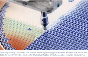
Siemens Digital Industries Software announced that Samsung Foundry’s advanced 3nm process technology now supports Siemens’ entire Calibre nmPlatform tool, which is the industry’s leading solution for physical verification of next-generation integrated circuits (ICs). With this certification, customers can now expand their utilization of the Calibre nmPlatform tool to leverage the extreme performance and power efficiency of Samsung’s leading-edge 3nm Gate All Around (GAA) process.
Siemens’ Calibre nmPlatform tool contains a broad array of physical verification technologies that IC design teams around the world rely on to generate sign-off quality IC designs, including Calibre nmDRC software, Calibre YieldEnhancer software, Calibre PERC software, Calibre xACT™ software and Calibre nmLVS software – all of which are now certified for Siemens’ bleeding-edge 3nm process.
“Siemens continues to demonstrate excellence in design enablement with the recent certification of its Calibre nmPlatform tool on Samsung Foundry’s latest 3nm process technology,” said Jongwook Kye, executive vice president of Design Enablement for Samsung Foundry. “Our close collaboration with Siemens is key to helping our mutual customers achieve silicon success with design solutions based on Samsung’s most advanced processes.”
Via certification of the sign-off versions of the Calibre platform design kits for Samsung’s 3nm process, mutual customers can now also use Siemens’ “shift-left” offerings from the Calibre portfolio, including the Calibre RealTime Custom software, Calibre RealTime Digital software (including the Calibre nmDRC-recon use model), and Calibre nmLVS-recon software tools. Engineered to help IC design teams and companies get to tapeout even faster, these solutions use sign-off Calibre design kits to help IC designers "shift left" their physical and circuit verification tasks by moving the identification, analysis, and resolution of complex IC and system-on-chip (SoC) physical verification issues into earlier stages of the design and verification flow, which can substantially speed-up time to closure.
Siemens and Samsung also collaborated closely during the development of the 3nm platform itself to help enable accurate parasitic modeling for Samsung’s 3nm Gate All Around process. The companies worked together so that, like the other Calibre offerings, the existing Siemens’ Calibre xACT software will work with Samsung GAA transistors.
Further, Samsung continues to use and leverage Calibre 3DSTACK and Calibre xACT software for 3DIC circuit verification, and has confirmed that the existing flows and capabilities continue to work effectively in systems including chiplets with 3nm GAA devices.
“Siemens is pleased to continue our collaboration with Samsung as they introduce their 3nm Gate All Around technology,” said Michael Buehler-Garcia, vice president of Calibre Design Solutions Product Management at Siemens Digital Industries Software. “As our mutual customers leverage Samsung’s 3nm offering to create higher level complexity designs, they can yet again be confident their Calibre software platform is already delivering the verification they need.
Samsung 3nm PDKs for Siemens’ Calibre software are available now from Samsung Foundry.


