MKS’ Atotech to Participate at ISES Taiwan 2022
October 11, 2022 | AtotechEstimated reading time: 1 minute

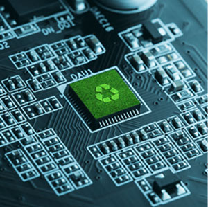
Atotech, a brand within the Materials Solutions Division of MKS Instruments, developing leading process and manufacturing technologies for next-generation power semiconductors and advanced packaging, joins the International Semiconductor Executive Summit (ISES Taiwan) in Hsinchu, Taiwan from October 11-12.
On Wednesday, October 12 from 9:30 a.m. – 9:45 a.m. CST, Dr. Christian Ohde, Global Director Semiconductor and Functional Electronics for MKS’ Atotech brand, will give the keynote and present on how technology pushes limits. His topic this year is “Plating solutions for next-generation power semiconductors and advanced packaging of highest reliability”.
During his talk, Dr. Ohde will elaborate on how the increasing functionality resulting from advanced node and packaging technologies as well as reliability requirements of power semiconductors go hand in hand with new requirements for the metallization processes. Furthermore, Dr. Ohde will explain the importance of fundamental R&D, which is the foundation to be equipped to provide next-generation chemistry and equipment solutions and meet the upcoming requirements of the semiconductor industry. He will discuss specific interconnect challenges, including higher stress sensitivity of smaller structures, the integration of heterogeneous structures, and new interconnect technologies to comply with higher interconnect density. He will also explain the path chosen for Atotech solutions when it comes to reliable copper, tailorable pillars, and low-temperature copper-to-copper direct bonding for smallest bonding solutions.
Suggested Items
RF PCB Design Tips and Tricks
05/08/2025 | Cherie Litson, EPTAC MIT CID/CID+There are many great books, videos, and information online about designing PCBs for RF circuits. A few of my favorite RF sources are Hans Rosenberg, Stephen Chavez, and Rick Hartley, but there are many more. These PCB design engineers have a very good perspective on what it takes to take an RF design from schematic concept to PCB layout.
Trouble in Your Tank: Causes of Plating Voids, Pre-electroless Copper
05/09/2025 | Michael Carano -- Column: Trouble in Your TankIn the business of printed circuit fabrication, yield-reducing and costly defects can easily catch even the most seasoned engineers and production personnel off guard. In this month’s column, I’ll investigate copper plating voids with their genesis in the pre-plating process steps.
Elephantech: For a Greener Tomorrow
04/16/2025 | Marcy LaRont, PCB007 MagazineNobuhiko Okamoto is the global sales and marketing manager for Elephantech Inc., a Japanese startup with a vision to make electronics more sustainable. The company is developing a metal inkjet technology that can print directly on the substrate and then give it a copper thickness by plating. In this interview, he discusses this novel technology's environmental advantages, as well as its potential benefits for the PCB manufacturing and semiconductor packaging segments.
Trouble in Your Tank: Organic Addition Agents in Electrolytic Copper Plating
04/15/2025 | Michael Carano -- Column: Trouble in Your TankThere are numerous factors at play in the science of electroplating or, as most often called, electrolytic plating. One critical element is the use of organic addition agents and their role in copper plating. The function and use of these chemical compounds will be explored in more detail.
IDTechEx Highlights Recyclable Materials for PCBs
04/10/2025 | IDTechExConventional printed circuit board (PCB) manufacturing is wasteful, harmful to the environment and energy intensive. This can be mitigated by the implementation of new recyclable materials and technologies, which have the potential to revolutionize electronics manufacturing.