


 It’s Only Common Sense: Stay Curious, My Friends
 The Marketing Minute: AI Is Watching Your Marketing Habits


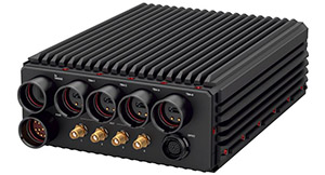
General Micro Systems (GMS), the world’s leading technology-independent supplier of computing engines in small form factors (SFF), boards and servers, today announced the launch of its X9 Spider family of distributed, ruggedized computing modules to support the demanding needs of next-generation warfare. Through its innovative inter-locking mechanical design, MOSA Thunderbolt™ interfaces, OpenVPX cross-platform compatibility, and patented LightBolt™ connectors, the X9 Spider family empowers designers to decentralize, distribute and rapidly upgrade computing, networking, storage, artificial intelligence (AI) and video resources wherever and however the program demands.
“Next-generation platforms like aircraft, vehicles, UAS and sensor systems require next-generation capabilities to maximize computing resources in lean, flexible and cost-effective ways,” said Ben Sharfi, chief architect and CEO, GMS. “By breaking the outdated and needlessly expensive, centralized ATR-style board-and-chassis paradigm into Thunderbolt™ technology-connected distributed compute modules, the X9 Spider family gives designers ruggedized, as-needed capabilities to solve any compute problem in any environment—from the smallest enclosure to the largest C5ISR system.” Rugged X9 Spider modules are small and modular, plug-and-play, and emphasize flexibility over ATR chassis’ physical and electrical constraints. An X9 module literally fits in the palm of your hand like a cell phone.
Built for limitless expandability, the X9 Spider family is based on brand-new, patent-pending mechanical features that allow devices to stack and connect together electrically, physically and thermally but at light speed (literally) with minimal signal bottlenecks. As well, X9 Spider connects directly to next-gen sensors without intermediate electronics—simplifying their connection to the electronic system—making the sensors themselves equally scalable and modular. This kind of upgradeability gives the DoD, primes and system developers limitless possibilities with very low upgrade costs.
No one in the rugged industry has anything like X9 Spider because much of the technology was invented and patented by GMS. The revolutionary family includes:
- Interconnectivity via the COTS open standard Thunderbolt™ 4 technology, developed by Intel® and Apple®. As well, 100Gb Ethernet over fiber connects X9 Spider modules to each other and to other high-speed systems
- Two “Host” modules with a range of storage and network capabilities powered either by Intel’s® latest 11th-generation Xeon W (Tiger Lake-H) 8-core CPU, or by NVIDIA’s® Jetson AGX Orin GPGPU with ARMcore engine, plus GPGPU CUDA and Tensor cores
- Six (6) companion X9 modules including: “Workstation” with removable storage and up to 14 sites for add-in I/O like MIL-STD-1553; Network “Switch” with four 100Gb and eight 10Gb Ethernet ports; “Storage” with removable canister and up to eight high-density M.2 or U.2 SSD storage devices; “GPGPU” with NVIDIA™ RTX-5000 GPGPU and custom I/O module such as video frame grabber for autonomous driver sensors; and utility X9 Spider modules for “Power” and “Cooler”
- Improved reliability and robustness through the patent-pending QuadroLock™ active wedge lock technology, enabling X9 Spider modules to interlock to withstand severe noise, vibration and harshness while simultaneously transferring heat between modules for maximum cooling
- Cutting-edge, long-range and cost-efficient interconnects through the patent-pending LightBolt™ connector, supporting Thunderbolt™ 4 fiber or copper and 100W power in one cable
The Achilles heel of a traditional ATR-style box using VME or OpenVPX cards is the lack of flexibility. The box can’t be opened or modified without a requalification; changing the cards requires I/O and backplane rewiring; upgrades can only be done using the box’s same card style (as opposed to choosing the market’s best technology choice); and the box is an expensive single point of failure. As well, with all functions centralized in one box, the whole system’s electrical power and heat is concentrated in one location.
“X9 Spider’s interoperability not only lowers acquisition costs, but it enables modernization and upgrade programs to move past restrictive single-box architectures like VME and OpenVPX and instead uses plug-and-play standards like Thunderbolt™ 4, 100Gigabit Ethernet and USB4 that are deployable anywhere on the platform,” Sharfi said. “This decentralizes computing, power distribution, and heat dissipation while improving fault tolerance through redundancy or merely by physically separating critical functions. These capabilities required new mechanical and electrical innovations to achieve a truly modular, distributed and scalable system that designers will love.”
The GMS X9 architecture includes 22 patents either filed for or granted.
Roll Out Begins Now for X9-Based Computing Engines, Designed and Made in America
The X9 Spider-based computing modules will be available in different variations to meet the unique needs of each application. The first module is the “X9 Spider Wearable”, also announced this week at AUSA2022. GMS will introduce other X9 Spider family products by the end of the year.
GMS has proudly designed and built X9 Spider in America—with the same design ethos as the company’s successful MIL-SPEC small form factor (SFF) computers, conduction-cooled servers, VME and VPX single-board computers, and rugged smart displays.


