


 Trouble in Your Tank: Causes of Plating Voids, Pre-electroless Copper
 Dan’s Biz Bookshelf: ‘Growth Hacker Marketing’
 Happy’s Tech Talk #38: Novel Metallization for UHDI


A Sneak Peak with Jim van den Hogen
December 29, 2022 | Andy Shaughnessy, Design007 MagazineEstimated reading time: 3 minutes
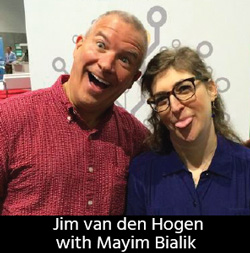
Jim van den Hogen has been teaching PCB designers and design engineers about fabrication processes for decades. Twenty years ago, I had the opportunity to see a class of his at PCB West; even back then, the room was jammed with designers eager to learn more about DFM techniques. Now Jim is bringing his teaching expertise to IPC APEX EXPO 2023 this January with a similar class directed at PCB designers. I asked Jim to give us a sneak peek into his curriculum and to share what he hopes attendees will take away from his class, as well as his thoughts on how to best bridge the gap between design and fabrication.
Andy Shaughnessy: Jim, tell us a little about your Professional Development class at IPC APEX EXPO 2023.
Jim van den Hogen: The class walks you through a basic multilayer fabrication process from front to back. It includes discussions on material, stackups, via metrics, aspect ratios, solder mask, surface finish, and various other fabrication-related topics. I have several sample sets that I’ll pass around for students to inspect. Each sample set has over 25 individual pieces, all of them taken at various steps of a multi-layer fabrication process, so students will be able to visualize the concepts we’ll be discussing in the class. We will also cover the typical requirements for a PCB fabrication drawing. The final portion of the class will cover array or manufacturing panel design, and ways to maximize cost savings when working with these processes.
Shaughnessy: Why should someone attend your class?
Van den Hogen: Students in my glass will gain a strong foundation in the basics of PCB fabrication and will get to go in-depth on the complexities of the process. You will learn how your design and specification thereof can affect the fabrication process and, in turn, how the delivered PCB can affect the assembly process.
Shaughnessy: It’s a fabrication class, but your target audience includes both PCB designers and design engineers. I know many designers who haven’t been in a board shop in decades, if at all; does that seem to be the case with your classes?
Van den Hogen: Yes, there are many designers and engineers that have never set foot in a board shop. It is difficult to understand the complexity of board fabrication without firsthand experience. While the PCB Fabrication Basics course presentation will get you close, a “behind the glass” board shop tour can tie it all together.
Shaughnessy: What is the most important piece of advice you give your attendees?
Van den Hogen: Engage with your suppliers up front. This becomes increasingly more important as your designs become more complex. Work with your supplier to define a fabrication stack-up that includes material selection, copper weights, plating thicknesses, and via/trace/space metrics. You will want to discuss what qualification specification(s) the finished product will need to meet. This may be an IPC specification (typically IPC-6012 and IPC-4101) or a corporate specification. This should be done as early in the design process as possible, preferably before you start placing parts in your design.
Shaughnessy: Is there anything else you’d like to add?
Van den Hogen: This class has been presented before and most of the attendee feedback comments mentioned how the sample sets that are passed out during class make it easier to grasp many of the topics presented. Also, while at the conference, you should plan on attending a standards development committee meeting. If you disagree with what is written or would like to help improve or update current specifications, that is where you’ll have your chance to make your voice heard.
Shaughnessy: Designers do like to share their opinions, so you may be in luck there. Thanks for talking with me, Jim.
Van den Hogen: Thank you, Andy.
Share on:


Suggested Items
Indium’s Karthik Vijay to Present on Dual Alloy Solder Paste Systems at SMTA’s Electronics in Harsh Environments Conference
05/06/2025 | Indium CorporationIndium Corporation Technical Manager, Europe, Africa, and the Middle East Karthik Vijay will deliver a technical presentation on dual alloy solder paste systems at SMTA’s Electronics in Harsh Environments Conference, May 20-22 in Amsterdam, Netherlands.
SolderKing Achieves the Prestigious King’s Award for Enterprise in International Trade
05/06/2025 | SolderKingSolderKing Assembly Materials Ltd, a leading British manufacturer of high-performance soldering materials and consumables, has been honoured with a King’s Award for Enterprise, one of the UK’s most respected business honours.
Knocking Down the Bone Pile: Gold Mitigation for Class 2 Electronics
05/07/2025 | Nash Bell -- Column: Knocking Down the Bone PileIn electronic assemblies, the integrity of connections between components is paramount for ensuring reliability and performance. Gold embrittlement and dissolution are two critical phenomena that can compromise this integrity. Gold embrittlement occurs when gold diffuses into solder joints or alloys, resulting in mechanical brittleness and an increased susceptibility to cracking. Conversely, gold dissolution involves the melting away of gold into solder or metal matrices, potentially altering the electrical and mechanical properties of the joint.
'Chill Out' with TopLine’s President Martin Hart to Discuss Cold Electronics at SPWG 2025
05/02/2025 | TopLineBraided Solder Columns can withstand the rigors of deep space cold and cryogenic environments, and represent a robust new solution to challenges facing next generation large packages in electronics assembly.
BEST Inc. Reports Record Demand for EZReball BGA Reballing Process
05/01/2025 | BEST Inc.BEST Inc., a leader in electronic component services, is pleased to announce they are experiencing record demand for their EZReball™ BGA reballing process which greatly simplifies the reballing of ball grid array (BGA) and chip scale package (CSP) devices.