


 It’s Only Common Sense: Stay Curious, My Friends
 The Marketing Minute: AI Is Watching Your Marketing Habits


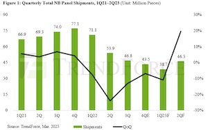
TrendForce estimates that shipments of display panels used in notebook computers (NB panels) will total 38.7 million pieces for 1Q23, showing a QoQ decline of 10.4% and a YoY decline of 45.6%. There are fewer work days for the first quarter due to the celebration of the Lunar New Year. Furthermore, brands for notebook computers (NBs) have been correcting down their panel orders in response to the issue of excess inventory. These factors were behind the significant contraction in shipments. However, TrendForce points out that the market for NB panels will improve in 2Q23. Besides more work days for the second quarter, brands will also have lowered their panel inventories to a manageable level by then. TrendForce currently forecasts that NB panel shipments will grow by 19.6% QoQ to a total of 46.3 million pieces for 2Q23.
The progress in the consumption of inventory for NB panels can be seen from the activities of the major NB brands (excluding Apple). Specifically, NB brands’ sales of whole devices and panel procurement quantities are the notable indicators. TrendForce has observed that the top five NB brands began to significantly cut panel demand in 2Q22 and kept making downward corrections through 2H22. Furthermore, their panel procurement quantities were kept lower than their device shipments. Hence, inventory was being steadily expended. TrendForce has also observed that the difference between the top five brands’ quarterly total device sell-in quantity and their quarterly total panel procurement quantity has been shrinking gradually over the recent three quarters.
Now, in 1Q23, some NB brands have lowered their inventories to an optimal for panels used in commercial NB models. However, several other brands have again scaled back their panel procurement quantities for the quarter because they still hold too many panels or whole devices for commercial NB models. Conversely, some brands have started to raise procurement quantities for panels used in consumer NB model. Therefore, TrendForce expects brands to have finished inventory correction by 2Q23. Furthermore, China’s domestic demand will likely warm up in the second quarter, and brands will be preparing for the “618” promotional event around the same time. TrendForce currently projects that NB panel shipments will return to a positive QoQ growth in 2Q23, thus ending five consecutive quarters of decline.
TrendForce believes NB sales on the whole will remain fairly weak during 1H23, but NB panels will be the first among different types of display panels to rebound in terms of shipments because most NB brands will have restored their panel inventories to a relatively healthy state within this period. Then, during 2H23, the US is expected to ease its interest rate hikes, and the inflation problem in Europe is also expected to subside. Additionally, China will likely experience a recovery in terms of the vigor of domestic socioeconomic activities following the lifting of COVID-19 lockdowns. With these factors, there is a high chance that NB panel shipments will return to the traditional seasonal cycle and surge during the busy season.


