


 Beyond the Board: What Companies Need to Know Before Entering the MilAero PCB Market
 Defense Speak Interpreted: If CHIPS Cuts Back, What Happens to Electronics Packaging Funds?
 American Made Advocacy: Where’s the Budget for a Modern Military Run on Microelectronics?


Insulectro and LCOA Install R&D Lab With Partner Kyocera in Orange County
March 7, 2023 | InsulectroEstimated reading time: 3 minutes
Insulectro, the largest distributor of materials for use in the manufacture of printed circuit boards and printed electronics, has opened a testing and development laboratory for Kyocera tools in its Lake Forest, California headquarters. The lab was created in association with backup and entry materials manufacturer LCOA in that company’s plant.
“I am pleased to announce that Insulectro, the exclusive North American distributor of drills, routers, endmills, and other cutting tools manufactured by Kyocera, will begin offering a variety of services from a new laboratory on our Lake Forest campus,” announced Geraldine Arseneau, Insulectro Product Manager for the Kyocera product line, “This will enable us to build on the synergy of Kyocera’s best-in-class tools and Insulectro’s dominance in drill room backup and entry products.” Arseneau joined Insulectro several years ago after a lengthy career with Kyocera.
The new lab is expected to support new product design, troubleshoot field issues, and include design feature testing, DoE (Design of Experiments) studies, confirmation testing, and repoint cycling testing.
It will determine proper feed and speed parameters for common PCB applications, develop processing parameters for new industry materials to understand how new technologies affect product performance, and supply customers with complete solutions. The Lab will also support industry and competitor benchmark studies.
Joe Negron, Kyocera Sales Manager, said, “The lab is a large next step for the Kyocera/Insulectro team. It vastly increases our capability to service our customers as technology changes.”
The Lab is equipped with a Schmoll drill/router (dual spindle drill with 160KRPM and router 50KRPM); a Microview CMM used to measure positional accuracy; and a Haas CM-1: compact CNC vertical machining center (50KRPM spindle, 5 HP motor).
It also includes a Struers automated polisher/grinder for X-sections; an Olympus Toolmakers microscope; and a metallograph to measure hole wall quality.
Insulectro Vice President of Product Management Michelle Walsh is also enthused about the additional capabilities, “This month we hosted a joint meeting of the Kyocera Team with Insulectro’s leadership and operations teams. We were all very excited not only about the Lab’s value for our existing customers but how we now have the capability to run studies to promote product offerings and qualifications requested by new customers. Fabricators can continue to count on Insulectro for the developing technological information.”
Kyocera SGS designs and manufactures tight tolerance precision carbide cutting tools for PCB applications. Products include drills, routers, end mills, and specialized cutting tools ranging from 0.05mm to 6.70mm diameters (0.0020" - 0.2638").
Kyocera’s renowned array of drills, routers, endmills, and specialty tools offer many benefits and advantages to customers for all their drilling and routing needs. Kyocera’s tool reliability and design flexibility are key strengths of their products, along with a complete R&D facility in the US, new tool manufacturing capability, and local technical resources, all available to support customer needs.
Insulectro supplies advanced engineered materials manufactured by Isola, DuPont, LCOA, CAC, Inc., Pacothane, Focus Tech, JX Nippon, TADCO, EMD Electronics (Ormet), Shikoku, Denkai America, ETI, Industrial Brush Corporation, Kyocera SGS Precision Tools, InduBond, and Shur-loc. These products are used by its customers to fabricate complex, multilayer circuit boards and to manufacture printed electronics components. Insulectro serves a broad customer base manufacturing rigid, rigid/flex, and flexible circuit boards for applications in a variety of end markets including aeronautics, telecom, data communications, high speed computing, mobile devices, military, and medical. Insulectro combines its premier product offering with local inventory across North America, fabrication capabilities and backed up by expert customer and technical support services.
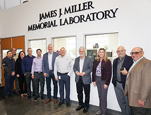
From Left to Right - Steve Komin, Senior Materials & Logistics Manager – Kyocera; Russ Reynoso, Design Engineering Manager – Kyocera; Geraldine Arseneau, Drill Product Manager – Insulectro; Curtis Vozar, Director of Material & Planning – Kyocera; Jeff Zaucha, Chief Financial Officer – Kyocera; Patrick Redfern, President & CEO – Insulectro; Dave Reiter, VP of Manufacturing – Kyocera; Tom Haag, President – Kyocera; Michelle Walsh, VP of Product Management – Insulectro; Joe Negron, Sales Manager PCB and MIT – Kyocera; Ken Parent, Chief Operating Officer – Insulectro.
Share on:


Testimonial
"We’re proud to call I-Connect007 a trusted partner. Their innovative approach and industry insight made our podcast collaboration a success by connecting us with the right audience and delivering real results."
Julia McCaffrey - NCAB GroupSuggested Items
Accelerating Embedded Innovation: Orthogone Becomes Texas Instruments Design Partner
09/17/2025 | PRNewswireOrthogone Technologies Inc., a leader in advanced embedded systems and FPGA development, is proud to announce its official designation as a Texas Instruments (TI) Design Services Partner.
BLT Joins Microchip Partner Program as Design Partner
09/17/2025 | BUSINESS WIREBLT, a U.S.-owned and operated engineering design services firm announced it has joined the Microchip Design Partner Program.
Staying on Top of Signal Integrity Challenges
09/16/2025 | Andy Shaughnessy, Design007 MagazineOver the years, Kris Moyer has taught a variety of advanced PCB design classes, both online IPC courses and in-person classes at California State University-Sacramento, where he earned his degrees in electrical engineering. Much of his advanced curriculum focuses on signal integrity, so we asked Kris to discuss the trends he’s seeing in signal integrity today, the SI challenges facing PCB designers, and his go-to techniques for controlling or completely eliminating SI problems.
American Standard Circuits to Exhibit and Host Lunch & Learn at PCB West 2025
09/17/2025 | American Standard CircuitsAnaya Vardya, President, and CEO of American Standard Circuits/ASC Sunstone Circuits has announced that his company will once again be exhibiting at PCB West 2025 to be held at the Santa Clara Convention Center on Wednesday, October 1, 2025.
ASM Technologies Limited signs MoU with the Guidance, Government of Tamilnadu to Expand Design-Led Manufacturing capabilities for ESDM
09/15/2025 | ASM TechnologiesASM Technologies Limited, a pioneer in Design- Led Manufacturing in the semiconductor and automotive industries, announced signing of Memorandum of Understanding (MoU) with the Guidance, Government of Tamilnadu whereby it will invest Rs. 250 crores in the state to expand its ESDM related Design-Led Manufacturing and precision engineering capacity. ASM Technologies will acquire 5 acres of land from the Government of Tamilnadu to set up a state-of-the-art design facility in Tamil Nadu's growing technology manufacturing ecosystem, providing a strong strategic advantage and long-term benefits for ASM.