











 The Chemical Connection: A Few Things That Still Scare Me
 The Right Approach: The Top 5 Scariest Things About AI in PCB Fabrication
 Punching Out: How Are the Big Boys Doing Now?






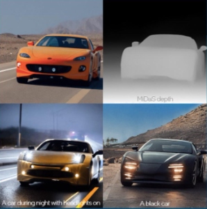
Depth estimation is a challenging computer vision task required to create a wide range of applications in robotics, augmented reality (AR) and virtual reality (VR). Existing solutions often struggle to correctly estimate distances, which is a crucial aspect in helping plan motion and avoiding obstacles when it comes to visual navigation. Researchers at Intel Labs are addressing this issue by releasing two AI models1 for monocular depth estimation: one for visual-inertial depth estimation and one for robust relative depth estimation (RDE).
The latest RDE model, MiDaS version 3.1, predicts robust relative depth using only a single image as an input. Due to its training on a large and diverse dataset, it can efficiently perform on a wider range of tasks and environments. The latest version of MiDaS improves model accuracy for RDE by about 30% with its larger training set and updated encoder backbones.
MiDaS has been incorporated into many projects, most notably Stable Diffusion 2.0, where it enables the depth-to-image feature that infers the depth of an input image and then generates new images using both the text and depth information. For example, digital creator Scottie Fox used a combination of Stable Diffusion and MiDaS to create a 360-degree VR environment. This technology could lead to new virtual applications, including crime scene reconstruction for court cases, therapeutic environments for healthcare and immersive gaming experiences.
Intel Introduces MiDaS 3.1 for Computer Vision
While RDE has good generalizability and is useful, the lack of scale decreases its utility for downstream tasks requiring metric depth, such as mapping, planning, navigation, object recognition, 3D reconstruction and image editing. Researchers at Intel Labs are addressing this issue by releasing VI-Depth, another AI model that provides accurate depth estimation.
VI-Depth is a visual-inertial depth estimation pipeline that integrates monocular depth estimation and visual-inertial odometry (VIO) to produce dense depth estimates with a metric scale. This approach provides accurate depth estimation, which can aid in scene reconstruction, mapping and object manipulation.
Incorporating inertial data can help resolve scale ambiguity. Most mobile devices already contain inertial measurement units (IMUs). Global alignment determines appropriate global scale, while dense scale alignment (SML) operates locally and pushes or pulls regions toward correct metric depth. The SML network leverages MiDaS as an encoder backbone. In the modular pipeline, VI-Depth combines data-driven depth estimation with the MiDaS relative depth prediction model, alongside the IMU sensor measurement unit. The combination of data sources allows VI-Depth to generate more reliable dense metric depth for every pixel in an image.