


 It’s Only Common Sense: Stay Curious, My Friends
 The Marketing Minute: AI Is Watching Your Marketing Habits


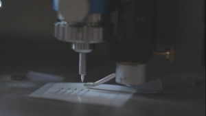
Engineers at Duke University have produced the world’s first fully recyclable printed electronics that replace the use of chemicals with water in the fabrication process. By bypassing the need for hazardous chemicals, the demonstration points down a path industry could follow to reduce its environmental footprint and human health risks.
The research appeared online Feb. 28 in the journal Nano Letters.
One of the dominant challenges facing any electronics manufacturer is successfully securing several layers of components on top of each other, which is crucial to making complex devices. Getting these layers to stick together can be a frustrating process, particularly for printed electronics.
“If you’re making a peanut butter and jelly sandwich, one layer on either slice of bread is easy,” explained Aaron Franklin, the Addy Professor of Electrical and Computer Engineering at Duke, who led the study. “But if you put the jelly down first and then try to spread peanut butter on top of it, forget it, the jelly won’t stay put and will intermix with the peanut butter. Putting layers on top of each other is not as easy as putting them down on their own — but that’s what you have to do if you want to build electronic devices with printing.”
In previous work, Franklin and his group demonstrated the first fully recyclable printed electronics. The devices used three carbon-based inks: semiconducting carbon nanotubes, conductive graphene and insulating nanocellulose. In trying to adapt the original process to only use water, the carbon nanotubes presented the largest challenge.
To make a water-based ink in which the carbon nanotubes don’t clump together and spread evenly on a surface, a surfactant similar to detergent is added. The resulting ink, however, does not create a layer of carbon nanotubes dense enough for a high current of electrons to travel across.
“You want the carbon nanotubes to look like al dente spaghetti strewn down on a flat surface,” said Franklin. “But with a water-based ink, they look more like they’ve been taken one-by-one and tossed on a wall to check for doneness. If we were using chemicals, we could just print multiple passes again and again until there were enough nanotubes. But water doesn’t work that way. We could do it 100 times and there’d still be the same density as the first time.”
This is because the surfactant used to keep the carbon nanotubes from clumping also prevents additional layers from adhering to the first. In a traditional manufacturing process, these surfactants would be removed using either very high temperatures, which takes a lot of energy, or harsh chemicals, which can pose human and environmental health risks. Franklin and his group wanted to avoid both.
In the paper, Franklin and his group develop a cyclical process in which the device is rinsed with water, dried in relatively low heat and printed on again. When the amount of surfactant used in the ink is also tuned down, the researchers show that their inks and processes can create fully functional, fully recyclable, fully water-based transistors.
Compared to a resistor or capacitor, a transistor is a relatively complex computer component used in devices such as power control or logic circuits and sensors. Franklin explains that, by demonstrating a transistor first, he hopes to signal to the rest of the field that there is a viable path toward making some electronics manufacturing processes much more environmentally friendly.
Franklin has already proven that nearly 100% of the carbon nanotubes and graphene used in printing can be recovered and reused in the same process, losing very little of the substances or their performance viability. Because nanocellulose is made from wood, it can simply be recycled or biodegraded like paper. And while the process does use a lot of water, it’s not nearly as much as what is required to deal with the toxic chemicals used in traditional fabrication methods.
According to a United Nations estimate, less than a quarter of the millions of pounds of electronics thrown away each year is recycled. And the problem is only going to get worse as the world eventually upgrades to 6G devices and the Internet of Things (IoT) continues to expand. So any dent that could be made in this growing mountain of electronic trash is important to pursue.
While more work needs to be done, Franklin says the approach could be used in the manufacturing of other electronic components like the screens and displays that are now ubiquitous to society. Every electronic display has a backplane of thin-film transistors similar to what is demonstrated in the paper. The current fabrication technology is high-energy and relies on hazardous chemicals as well as toxic gasses. The entire industry has been flagged for immediate attention by the US Environmental Protection Agency.
“The performance of our thin-film transistors doesn’t match the best currently being manufactured, but they’re competitive enough to show the research community that we should all be doing more work to make these processes more environmentally friendly,” Franklin said.


