
















 It’s Only Common Sense: When the Cheapest Board Becomes the Most Expensive
 The Chemical Connection: Employee and Operator Empowerment in the Age of AI
 The Big Picture: Not One, But Three Grey Rhinos





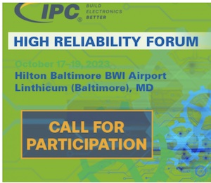
IPC is now accepting abstracts for the High Reliability Forum, the international conference focusing on Class 3 and safety critical electronics for mil-aero, automotive, medical, and long-life applications that are subjected to harsh use environments. The High Reliability Forum will be held October 17-19, 2023, at the Hilton Baltimore BWI Airport in Linthicum (Baltimore), Md.
IPC invites innovators and technologists to submit an abstract for a technical presentation during the conference. The IPC High Reliability Technical Forum Program Committee seeks proposals for technical presentations on the following topics:
- High Reliable Materials: PCB Fabrication Materials, Interconnecting, Bonding, Thermal/Power Management, Conductivity/Resistivity, Use Conditions/Environment (A&D vs. Automotive vs. Medical/Implantable vs. High Perf Computing, etc.), Environmental Restrictions/Impact, Substrates for Advanced Packaging
- Design and Fabrication for High Reliability: Materials Compatibility, Flexible Printed Boards in RF/Microwave Applications, Design for Reliability/Determining Reliability Requirements, System of Systems Architecture, Levels of Redundancy, HDI/Microvia Reliability -- Test Methods and Design Rules, Micro HDI and Substrate Technologies, First Level Interconnect Methodologies; Use of Simulation in the Design Process, Automotive/High Voltage Applications
- Assembly for High Reliability: Next Generation Solder Alloys, Solder Paste and Coating Selection for High Reliability, Reliability of Cleaning, Testing and Coating Strategies, Assembly Materials -- Coating, Cleaning, Underfilling, Encapsulation, Effects of No-Clean Residues, Voiding in Solder Joints, 3D Package Level Reliability, Assembly for Automotive/High Voltage Applications
- Testing for High Reliability: Fatigue Behavior and Reliability Testing for Solder Joints using Next Generation Solder Alloys, Harsh Environment Reliability and Testing, Thermal Stress Test Methods, Connector Failure Modes and Reliability, Vibration and Shock Test Methods for Predicting Reliability, HDI/Microvia Reliability, Automotive/High Voltage Applications, Heterogeneous Integration/Advanced Packaging for High Reliability
- Issues around Quality, Standards for High Reliability: Supply Chain, Reshoring/Onshoring, Failure Modes Effects Analysis (FMEA), Reliability Assurance and Prediction Workflows, Selection of Appropriate Class of Electronics, Requirements for Specific Class of Electronics, Manufacturing Standards, Emerging Electronic Technologies
“We are thrilled to welcome attendees back to the first High Reliability Forum since 2019,” said David Bergman, IPC vice president of standards and technology. “We are eager to see the exciting new work from experts in all areas of the industry including PCB design, fabrication materials, emerging technologies, and other applications with specialized reliability requirements.”
Abstracts summarizing original and previously unpublished work must be submitted for consideration to present. Presentations should be non-commercial and describe significant results from experiments, emphasize new techniques, discuss trends of interest, and contain technical and/or appropriate test results.
Abstracts are due on Monday, June 5, 2023 and will be peer-reviewed by the Technical Program Committee. Accepted abstracts will be invited to deliver a podium presentation in person at the High Reliability Forum in Linthicum Heights, Maryland, October 17-19, 2023.


