


 It’s Only Common Sense: Stay Curious, My Friends
 The Marketing Minute: AI Is Watching Your Marketing Habits


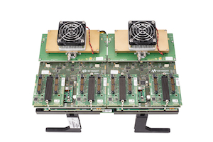
Keysight Technologies, Inc. released a new Universal Signal Processing Architecture (USPA) prototyping platform, enabling semiconductor companies to conduct complete chip prototyping and verification, pre-tapeout, in a real-time development environment integrating digital twins of fully-compliant, standards-based signals.
The final step of the chip design process, known as the silicon tapeout, is an increasingly expensive procedure that leaves little room for design failure. If a design fails following the tapeout, chip makers must start over again with a new “re-spin” that can take 12 months or longer to complete. In addition to tying up valuable research and development resources, these chip redesigns can potentially cause the chip maker to miss a narrow time-to-market window.
To reduce the risks of design failures and expensive re-spins, the Keysight USPA platform provides chip designers and engineers with complete digital twin signaling to verify designs before they are committed to silicon. The USPA platform offers designers an alternative to proprietary custom prototyping systems by integrating ultrafast signal converters with a high performance, completely modular field-programmable gate array (FPGA) prototyping system.
The unique USPA prototyping platform offers the following benefits:
- Supports the highest performance optoelectronic development projects with digital-to-analog converter (DAC) and analog-to-digital converter (ADC) interfaces that emulate signals at full speed, up to 68 GS/s (ADC) and 72 GS/s (DAC).
- Provides a broad range of input / output interfaces that are suitable for applications including 6G wireless development, digital radio frequency memory, advanced physics research, and high-speed data acquisition applications, such as radar and radio astronomy.
- Offers flexibility with two configurations, including a pre-configured system for single channel transceiver applications and a fully configurable set of modular components that can be combined to support a wide range of single and multi-channel applications. In addition, the pre-configured system can be expanded with additional components that leverage the modularity, scalability, and cost-effective reusability of the platform architecture.
Hong Jiang, CEO Avance Semi, Inc., said: “When we began work on our first ASIC for the coherent fiber communication market, we understood that we might only have one chance to get it right and that a second tapeout would be both prohibitively expensive and so time-consuming that we could miss our narrow time-to-market window. With Keysight’s USPA platform and our system integration effort, we can optimize and verify our design in real-time as it progresses. This is like a ‘free soft tapeout’ we can run as many times as needed. This approach saves development time and money while dramatically increasing confidence in our design and product release timeline.”
Dr. Joachim Peerlings, Vice President and General Manager of Keysight’s Network and Data Center Solutions Group, said: “By accelerating and de-risking chip development, Keysight USPA delivers a new end-to-end solution that meets the challenges of leading-edge designs in a very high-cost environment. This powerful platform gives chip developers a digital twin of their future silicon device, allowing them to fully validate their designs and algorithms before incurring the expense and risk of a tapeout.”


