


 Beyond the Board: Early Engagement Means Faster Prototyping for Defense Programs
 Defense Speak Interpreted: The Autonomous Plane Battle—Skyborg Vs. Loyal Wingman
 American Made Advocacy: Congress Back from Break With Work To Do


MKS Introduces ESI Geode A CO2 Laser System for High Precision and High-Speed ABF IC Substrate Manufacturing
May 31, 2023 | MKS Instruments, Inc.Estimated reading time: 1 minute
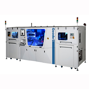
MKS Instruments, Inc., a global provider of technologies that transform our world, announced the official launch of the ESI Geode® A laser drill system today, a new configuration of the Geode® platform designed explicitly for drilling vias in the non-copper-clad ABF substrate market.
The Geode® A laser drilling system provides processing and application solutions for the FCBGA package substrate market, components which provide critical building blocks for everyday electronic devices and, in particular, high-performance computing. FCBGA substrates help enable supercomputing, artificial intelligence processing, autonomous cars, and other highly complex semiconductor modules.
“Manufacturers are under increased market pressure to deliver components that meet the precise demands of miniaturization and complexity required for advanced substrate manufacturing. At MKS, we are keenly focused on delivering the advanced technology needed for our customers to deliver next-generation productivity and quality,” said John Williams, MKS Vice President and General Manager of the ESI business. “In addition, the Geode® A laser drill is engineered as an integral component to the MKS Optimize the Interconnect SM solution, combining ESI laser drilling technologies with Atotech chemistry and plating equipment to provide customers with a full package of via formation technologies required to deliver optimal quality with the highest productivity for PCB and package substrate products.”
The Geode® A laser drilling system combines an innovative laser and optics configuration with precision pulse-shaping and beam-steering designed for ABF materials. These engineering innovations deliver the lowest cost of ownership and a greener manufacturing solution through 21% less floor space utilization, 72% less weight, and up to 65% less power consumption than the competition.
The Geode® A laser drilling system is available for purchase. More details can be found at www.esi.com, and system experts will be available at the JPCA 2023, Tokyo, Japan, May 31-June 2 in booth 6B-11.
Share on:


Testimonial
"The I-Connect007 team is outstanding—kind, responsive, and a true marketing partner. Their design team created fresh, eye-catching ads, and their editorial support polished our content to let our brand shine. Thank you all! "
Sweeney Ng - CEE PCBSuggested Items
Episode 6 of Ultra HDI Podcast Series Explores Copper-filled Microvias in Advanced PCB Design and Fabrication
10/15/2025 | I-Connect007I-Connect007 has released Episode 6 of its acclaimed On the Line with... American Standard Circuits: Ultra High Density Interconnect (UHDI) podcast series. In this episode, “Copper Filling of Vias,” host Nolan Johnson once again welcomes John Johnson, Director of Quality and Advanced Technology at American Standard Circuits, for a deep dive into the pros and cons of copper plating microvias—from both the fabricator’s and designer’s perspectives.
Nolan’s Notes: Tariffs, Technologies, and Optimization
10/01/2025 | Nolan Johnson -- Column: Nolan's NotesLast month, SMT007 Magazine spotlighted India, and boy, did we pick a good time to do so. Tariff and trade news involving India was breaking like a storm surge. The U.S. tariffs shifted India from one of the most favorable trade agreements to the least favorable. Electronics continue to be exempt for the time being, but lest you think that we’re free and clear because we manufacture electronics, steel and aluminum are specifically called out at the 50% tariff levels.
MacDermid Alpha & Graphic PLC Lead UK’s First Horizontal Electroless Copper Installation
09/30/2025 | MacDermid Alpha & Graphic PLCMacDermid Alpha Electronics Solutions, a leading supplier of integrated materials and chemistries to the electronics industry, is proud to support Graphic PLC, a Somacis company, with the installation of the first horizontal electroless copper metallization process in the UK.
Electrodeposited Copper Foils Market to Grow by $11.7 Billion Over 2025-2032
09/18/2025 | Globe NewswireThe global electrodeposited copper foils market is poised for dynamic growth, driven by the rising adoption in advanced electronics and renewable energy storage solutions.
MacDermid Alpha Showcases Advanced Interconnect Solutions at PCIM Asia 2025
09/18/2025 | MacDermid Alpha Electronics SolutionsMacDermid Alpha Electronic Solutions, a global leader in materials for power electronics and semiconductor assembly, will showcase its latest interconnect innovations in electronic interconnect materials at PCIM Asia 2025, held from September 24 to 26 at the Shanghai New International Expo Centre, Booth N5-E30