


 The Marketing Minute: Marketing With Layers
 The Right Approach: Electro-Tek—A Williams Family Legacy, Part 1
 It’s Only Common Sense: If You’re Not Differentiated, You’re Dead


Nanusens Secures First IP License for MEMS-in-ASICs Sensor Technology
June 15, 2023 | NanusensEstimated reading time: 1 minute
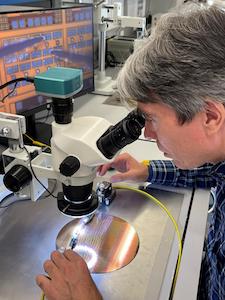
Nanusens, a fabless semiconductor company supplying novel MEMS sensors built inside CMOS, has announced the first IP license agreement for its MEMS-in-ASICs technology with Azoteq, a pioneer in high volume sensor fusion ICs used in industrial and consumer applications.
Nanusens technology enables its MEMS (Micro Electro Mechanical Systems) IP sensor structures to be made at the same time within a chip as other IP on the ASIC using standard CMOS processes, resulting in ASICs with embedded MEMS sensors. This breakthrough of the integration of sensor solutions as IP blocks offers dramatic reductions in costs and size as it completely replaces the current solution of discrete sensor packages.
Dr Josep Montanyà, CEO of Nanusens, said, “Azoteq is one of a number of companies that recently received samples of our 3D accelerometer that were created using an IP block within an ASIC. Azoteq is the first to sign an IP license and we plan to announce several more license deals soon.”
Dr Dieter Mellet, Azoteq’s CTO, commented, “Our business is based on creating multi-sensor solutions for customers who often need to include many sensors into space-constrained applications. Nanusens technology enables monolithic integration of MEMS within an IC and is perfect for us as we can now embed an array of 3D accelerometers into an existing IC, providing cost, power and space saving to our customers over current solutions available today further expanding our ProxFusion® offering.”
Share on:


Testimonial
"The I-Connect007 team is outstanding—kind, responsive, and a true marketing partner. Their design team created fresh, eye-catching ads, and their editorial support polished our content to let our brand shine. Thank you all! "
Sweeney Ng - CEE PCBSuggested Items
Circus SE Set for High-Volume Market Entry in the Defense Sector
10/17/2025 | BUSINESS WIRECircus SE a global technology leader in AI robotics for autonomous nutrition systems and troop supply, is expanding its global production network as part of its high-volume market entry into the defense sector.
China Expands Rare Earth Export Restrictions, Tightening Grip on Global Supply Chains
10/16/2025 | I-Connect007 Editorial TeamChina sharply expanded its rare earth export restrictions on Oct. 9, adding additional elements and refining technologies to its control list while imposing stricter rules on foreign users in the defense and semiconductor industries.
SAMI Advanced Electronics Company Launches “Remal” Computer Manufacturing Project in Partnership with HP and Foxconn
10/15/2025 | SAMI-AECSAMI Advanced Electronics Company (SAMI-AEC), a wholly owned subsidiary of Saudi Arabian Military Industries (SAMI), proudly announced the launch of the “Remal” project for computer manufacturing, in strategic partnership with HP and Foxconn.
The Right Approach: Electro-Tek—A Williams Family Legacy, Part 1
10/15/2025 | Steve Williams -- Column: The Right ApproachThere is no bronze bust in the lobby or portrait in the conference room of Electro-Tek's founder—my Dad, Charles “Chuck” Williams—so with the facility closing last year after 56 years, I feel it is time to tell the story. Chuck Williams founded Electro-Tek in 1968 in our basement, eventually moving into the second floor of an old 1913 building in downtown Milwaukee that is still standing (the first of three eventual facilities).
LPKF Joins productronica’s 50th Anniversary, Showcasing Laser Technology for Electronics Manufacturing
10/10/2025 | LPKF Laser & ElectronicsLPKF Laser & Electronics invites visitors to productronica 2025 in Munich from November 18 to 21. At booth 305 in hall B2, the company will present its portfolio of modern laser technologies for the electronics industry live – from prototyping systems and high-performance depaneling to laser plastic welding for electronic housings and thin glass processing for advanced packaging.