Ansys Simulation Boosts Thermal Reliability of uPI's Power Management Products by 100%
July 20, 2023 | PRNewswireEstimated reading time: 1 minute

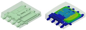
uPI Semiconductor Corp. (uPI) applies Ansys' simulation solutions to speed up design for its product packaging solutions and improve thermal reliability by 2X. uPI is a leading supplier of semiconductor power management chips for high-performance computing (HPC) applications, communications hardware, battery management, industrial equipment, and consumer products.
By leveraging Ansys simulation, uPI can predict the electrical, mechanical, and thermal characteristics of its high-performance chip package designs quickly and with predictive accuracy. This leads to improved product performance, streamlined design, and reduced risk of late-stage design changes. Using Ansys to analyze heat flow and thermomechanical stresses, uPI optimizes their package designs and doubles thermal reliability. Products that initially failed after 500 thermal test cycles were optimized with Ansys solutions to endure more than 1,000 cycles.
"Ansys' multiphysics simulation solutions enable uPI to optimize our chip package designs and dramatically improve product reliability," said Mr. Zhuang, packaging R&D manager at uPI. "With critical insights from Ansys' simulation tools into electrical, thermal, and structural characteristics, our teams have accelerated development and verification while significantly improving efficiency, reducing design errors, and enhancing product quality."
Ansys simulation tools also predict the electrical characteristics of packages across a range of signal frequencies, which helps uPI engineers identify optimal design solutions and improve product performance.
"Chip package design involves complex, multidimensional engineering that is nonlinear and can behave unexpectedly, even for small changes," said John Lee, vice president and general manager of the electronics, semiconductor, and optics business unit at Ansys. "Ansys' simulation tools provide end-to-end multiphysics analyses that enable teams to gain insight quickly into multiple areas of chip packaging with predictive accuracy. With Ansys, uPI is able to maximize their R&D and reliability testing processes to achieve high-quality products."
Testimonial
"Advertising in PCB007 Magazine has been a great way to showcase our bare board testers to the right audience. The I-Connect007 team makes the process smooth and professional. We’re proud to be featured in such a trusted publication."
Klaus Koziol - atgSuggested Items
Setting Design Constraints Effectively
07/31/2025 | Stephen V. Chavez, Siemens EDAPCB design requires controlling energy within the medium of a PCB. The manner in which we control the chaos of energy is by implementing and utilizing physical and electrical rules, known as constraints, along with a specific structure and material(s) that make up what is known as the foundation of the design. These rules govern everything within the PCB structure and generally fall into two camps: performance and manufacturability. Setting this foundation correctly is extremely important and the key to success.
MacDermid Alpha Electronics Solutions Unveils Unified Global Website to Deepen Customer, Talent, and Stakeholder Engagement
07/31/2025 | MacDermid Alpha Electronics SolutionsMacDermid Alpha Electronics Solutions, the electronics business of Elements Solutions Inc, today launched macdermidalpha.com - a unified global website built to deepen digital engagement. The launch marks a significant milestone in the business’ ongoing commitment to delivering more meaningful, interactive, and impactful experiences for its customers, talent, and stakeholders worldwide.
Ansys 2025 R2 Enables Next-Level Productivity by Leveraging AI, Smart Automation, and Broader On-Demand Capabilities
07/30/2025 | PRNewswireAnsys, now part of Synopsys, announced 2025 R2, featuring new AI-powered capabilities across the portfolio that accelerate simulation and expand accessibility.
Connect the Dots: Sequential Lamination in HDI PCB Manufacturing
07/31/2025 | Matt Stevenson -- Column: Connect the DotsAs HDI technology becomes mainstream in high-speed and miniaturized electronics, understanding the PCB manufacturing process can help PCB design engineers create successful, cost-effective designs using advanced technologies. Designs that incorporate blind and buried vias, boards with space constraints, sensitive signal integrity requirements, or internal heat dissipation concerns are often candidates for HDI technology and usually require sequential lamination to satisfy the requirements.
Target Condition: The 5 Ws of PCB Design Constraints
07/29/2025 | Kelly Dack -- Column: Target ConditionHave you ever sat down to define PCB design constraints and found yourself staring at a settings window with more checkboxes than a tax form? You’re not alone. For many designers—especially those newer to the layout world—the task of setting up design constraints can feel like trying to write a novel in a language you just started learning.