


 Trouble in Your Tank: Interconnect Defect—The Three Degrees of Separation
 It’s Only Common Sense: Creating a Company Culture Rooted in Well-being
 Dan’s Biz Bookshelf: ‘Notorious: Leadership Lessons from History’s Most Notorious Leaders’
JEOL Introduces Two New Scanning Electron Microscopes at M&M 2023
July 24, 2023 | JEOLEstimated reading time: 1 minute
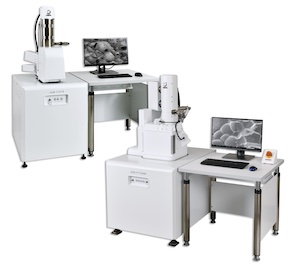
JEOL introduces two new Scanning Electron Microscopes this week at M&M 2023 in Minneapolis. The new SEMs incorporate the next level of intelligent technology and automation for ease of operation and fast, high-resolution imaging and analysis. These new-generation SEMs make it easy to acquire data for all specimen types.
Both new SEMs feature “Simple SEM” for automatic image collection at multiple locations, magnifications, and conditions, Live EDS analysis, Live 3D microscopy, automatic large-area analysis with ZeroMag software, Montage for large area mosaics, and automatic functions from alignment to focus for fast, clear, high-resolution images.
The new JSM-IT710HR SEM is a compact, versatile Schottky Field Emission SEM that delivers large probe currents while maintaining a small probe, making it ideally suited for higher resolution needs. A large specimen chamber and both High and Low Vacuum operation allow a wide variety of specimen types to be imaged and analyzed in their native state.
The new JSM-IT210 InTouchScopeTM SEM is a compact microscope with easy, automated workflow features including Specimen Exchange mode that guides a new operator step-by-step from sample introduction to ideal imaging and analysis conditions.
JEOL has a complete range of Scanning Electron Microscopes ranging from the popular NeoScope tabletop SEM to its flagship ultrahigh resolution field emission SEM. JEOL offers applications and service support for all of its Electron Microscopes and scientific instruments, with over 70 years of expertise in electron optics.
Share on:


Suggested Items
Connect the Dots: Designing for Reality—Outer Layer Imaging
09/26/2024 | Matt Stevenson -- Column: Connect the DotsWelcome to the next step in the manufacturing process—the one that gets the chemical engineer in all of us excited. I am referring to outer layer imaging, or how we convert digital designs to physical products. On a recent episode of I-Connect007’s On the Line with… podcast, we explained how the outer layer imaging process maps the design’s unique features onto the board.
Omni Design Technologies Partners with Aura Intelligent Systems on Next Generation Radar
09/16/2024 | BUSINESS WIREOmni Design Technologies, a leading provider of high-performance, low-power data acquisition and signal-processing solutions, and Aura Intelligent Systems, a developer of high-resolution imaging radar for ADAS and autonomous vehicles, announced a partnership on Aura’s next generation digital radar development.
MEMS & Imaging Sensors Summit to Highlight Innovations Driving the Next Generation of Connectivity
09/11/2024 | SEMIThe SEMI MEMS & Imaging Sensors Summit, themed Sensor Revolution for a Connected Future, is set to bring together some of the world’s leading minds in sensor technology on November 14 at the International Conference Center Munich (ICM), Germany.
Teledyne FLIR Delivering Airborne Surveillance Systems to Japan Maritime Self-Defense Force Worth Up to $21 Million
09/09/2024 | BUSINESS WIRETeledyne FLIR Defense, part of Teledyne Technologies Incorporated, has announced that it is delivering its Star SAFIRE® 380-HLD multi-spectral imaging systems to the Japan Maritime Self-Defense Force (JMSDF) as part of an agreement worth up to $20.8 million.
Schmoll America: Thriving in the Global PCB Market
07/31/2024 | Marcy LaRont, PCB007 MagazineAs we examine what it means to thrive in our industry, I reached out to Kurt Palmer, president of Schmoll America. The business expansion was created from Schmoll Maschinen to focus on and better serve the expanding North American PCB market. Professionally, Kurt has been in this business for decades. He explains what thriving looks like for Schmoll America as the company moves forward into this new venture and what he is most looking forward to in the years ahead.