


 Beyond the Board: What Companies Need to Know Before Entering the MilAero PCB Market
 Defense Speak Interpreted: If CHIPS Cuts Back, What Happens to Electronics Packaging Funds?
 American Made Advocacy: Where’s the Budget for a Modern Military Run on Microelectronics?


Analog Devices Invests More Than $1 Billion in Semiconductor Facility Expansion in Oregon
July 28, 2023 | Analog Devices, Inc.Estimated reading time: 2 minutes
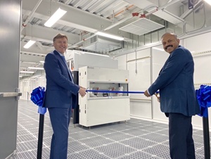
Analog Devices, Inc., a global semiconductor leader, celebrated its more than $1 billion investment to expand its semiconductor wafer fab in Beaverton, Oregon. The Beaverton site, built in 1978, is ADI’s largest wafer fabrication facility by volume and serves customers in critical industries, such as industrial, automotive, communications, consumer, and healthcare.
The facility investment expands cleanroom space to about 118,000 sq-ft and nearly doubles internal manufacturing of products running on the 180-nanometer technology node and above. It is also expected to create hundreds of new, long-term employment opportunities, a significant increase to ADI’s current roughly 950 employees in Oregon.
More than 10% of the total investment is for new, state-of-the-art fab tools intended to increase overall efficiency and utilize chemistries that are more environmentally friendly. Despite nearly doubling production output, the facility is targeting to reduce absolute greenhouse gas emissions by approximately 75% and water usage per production unit by approximately 50%.
"By expanding ADI’s Beaverton facility, we are increasing our production capacity in critical industries, boosting domestic manufacturing in line with the vision of the CHIPS Act, and enhancing the global resiliency of ADI’s hybrid manufacturing model," said Vincent Roche, ADI’s CEO and Chair. "While our investment in Beaverton will facilitate these goals, they will be achieved through the incredible dedication and talent of ADI's existing workforce and further tapping into Oregon's strong talent pool."
Commenting on the announcement, U.S. Senator Ron Wyden of Oregon said, “Today’s good news from Analog Devices marks a significant step to ensure Oregon is taking full advantage of the federal CHIPS Act I worked to pass into law. This announcement strengthens a signature industry in Oregon by solidifying semiconductors’ place in the Silicon Forest and beyond, creating statewide impact with new good-paying jobs in Beaverton and rippling out to benefit the entire state economy.”
In addition, the Beaverton facility will host the Semiconductor Advanced Manufacturing University (SAMU), a workforce development training center that will offer eight-week courses to train groups of around 25 students each on semiconductor equipment maintenance. A key driver of ADI’s efforts with the training center is providing training opportunities to many diverse groups within the local community, including U.S. military veterans, people re-entering the workforce, and existing ADI factory operators, to learn semiconductor manufacturing fundamentals and other curriculum to advance their professional development.
ADI’s hybrid manufacturing model is a broad network of internal factories and external partners. This model enables effective management of ADI operations through economic cycles, enhances the resiliency of its global supply chain, and better serves its customer needs. To improve ADI-owned operations, the company has increased capital investment to a high single-digit percent of revenue in fiscal year 2022 and to date in fiscal year 2023 from its historical precedent of around four percent. These manufacturing investments span the globe, including in the states of Washington and Massachusetts, as well as in Ireland, Thailand, Malaysia, and the Philippines.
Share on:


Testimonial
"We’re proud to call I-Connect007 a trusted partner. Their innovative approach and industry insight made our podcast collaboration a success by connecting us with the right audience and delivering real results."
Julia McCaffrey - NCAB GroupSuggested Items
Electrodeposited Copper Foils Market to Grow by $11.7 Billion Over 2025-2032
09/18/2025 | Globe NewswireThe global electrodeposited copper foils market is poised for dynamic growth, driven by the rising adoption in advanced electronics and renewable energy storage solutions.
iDEAL Semiconductor Announces Polar Semiconductor as Manufacturing Partner for SuperQ™ Power Devices
09/18/2025 | PRNewswireiDEAL Semiconductor confirms that its ultra-efficient SuperQ™ silicon power devices are now in production at Polar Semiconductor, a leading foundry specializing in high-voltage, power, and sensor technologies.
U.S. Manufacturing Jobs Decline Amid Tariffs and Immigration Crackdown
09/17/2025 | I-Connect007 Editorial TeamManufacturers in the U.S. are cutting jobs even as President Donald Trump pushes policies he says will revitalize the industry. Employers shed 12,000 manufacturing jobs in August, while payrolls in the sector have fallen by 42,000 since April, according to a new analysis from the Center for American Progress (CAP) based on government labor data.
Richardson Electronics Appoints Daniel Albers to Drive Made-in-USA Contract Manufacturing Expansion
09/17/2025 | Globe NewswireRichardson Electronics, Ltd., a global provider of engineered solutions for the green energy, power management, and custom display markets, announced the appointment of Daniel Albers to spearhead business development for its expanded, Made-in-USA contract manufacturing efforts.
GlobalFoundries Joins World Economic Forum’s Global Lighthouse Network for Manufacturing Excellence
09/17/2025 | GlobalFoundriesGlobalFoundries announced that the World Economic Forum (WEF) has designated its 300mm fab in Singapore as part of the Global Lighthouse Network (GLN) of advanced manufacturers.