


 Global PCB Connections: Rigid-flex and Flexible PCBs—The Backbone of Modern Electronics
 Flexible Thinking: The Key to a Successful Flex Circuit Design Transfer
 Happy’s Tech Talk #29: Bend-to-Install Semi-flex FR-4


Revolutionary X-Ray Microscope Unveils Sound Waves Deep Within Crystals
October 10, 2023 | SLAC National Accelerator LaboratoryEstimated reading time: 2 minutes
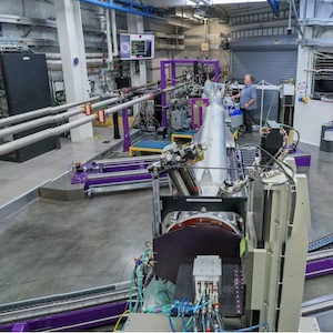
Researchers at the Department of Energy’s SLAC National Accelerator Laboratory. Stanford University, and Denmark Technical University have designed a cutting-edge X-ray microscope capable of directly observing sound waves at the tiniest of scales – the lattice level within a crystal. These findings, published last week in Proceedings of the National Academy of Sciences, could change the way scientists study ultrafast changes in materials and the resulting properties.
“The atomic structure of crystalline materials gives rise to their properties and associated ‘use-case’ for an application,” said one of the researchers, Leora Dresselhaus-Marais, an assistant professor at Stanford and SLAC. “The crystalline defects and atomic scale displacements describe why some materials strengthen while others shatter in response to the same force. Blacksmiths and semiconductor manufacturing have perfected our ability to control some types of defects, however, few techniques today can image these dynamics in real-time at the appropriate scales to resolve how those the distortions connect to the bulk properties.”
In this new work, the team generated soundwaves in a diamond crystal, then used the new X-ray microscope they developed to directly image the subtle distortions inside the crystalline lattice. They did so at the timescales at which these atomic-scale vibrations naturally occur by leveraging the ultrafast and ultrabright pulses available at SLAC’s Linac Coherent Light Source (LCLS).
The researchers placed a special X-ray lens along the beam diffracted by the crystalline lattice to filter out the “perfectly packed” portion of the crystal and zero in on distortions in the crystal's structure caused by the sound wave and defects.
“We used this to image how an ultrafast laser transfers its light energy into heat via successive reflections of the out-of-equilibrium sound wave off the front and back surface of the crystal.” Dresselhaus-Marais said. “By showing this in diamond – a crystal with the fastest sound speed – we illustrate the new opportunities now available with our microscope to study new phenomena deep inside crystals.”
The results identify a way to see super-fast changes in materials without damaging them. Before this discovery, the tools researchers used were much too slow to see these changes. This matters because many things, like how heat moves or how sound waves spread, depend on these fast changes.
The implications of this breakthrough stretch across various disciplines, from materials science to physics, and even extend to fields like geology and manufacturing. By understanding the atomic-level changes that lead to larger observable events in materials, scientists can get a clearer picture of transformations, melting processes, and chemical reactions in materials – accessing a new 13 orders of magnitude of timescales.
“This new tool offers us a unique opportunity to study how rare events caused by defects, atomic-distortions, or other localized stimuli inside a lattice give rise to macroscopic changes in materials,” Dresselhaus-Marais said. “While our understanding of the macroscopic changes in materials is rather advanced, we are often missing the details of which ‘instigating events’ ultimately cause the phase transformations, melting, or chemistry we observe at larger scales. With ultrashort timescales now at our fingertips, we have the ability to hunt for these rare events at their native timescales.”
Share on:


Testimonial
"Advertising in PCB007 Magazine has been a great way to showcase our bare board testers to the right audience. The I-Connect007 team makes the process smooth and professional. We’re proud to be featured in such a trusted publication."
Klaus Koziol - atgSuggested Items
SEMI Foundation Honors Applied Materials at SEMICON West with 2025 Excellence in Achievement Award for Talent Development
11/04/2025 | SEMIThe SEMI Foundation announced it recognized Applied Materials, Inc. with the Excellence in Achievement Award at SEMICON West 2025 in Phoenix, Arizona, honoring the company’s outstanding leadership and collaboration in building the next generation of semiconductor talent.
Sealed for Survival: Potting Electronics for the Toughest Environments
10/29/2025 | Beth Massey, MacDermid Alpha Electronics SolutionsElectronics deployed in harsh conditions face relentless threats from vibration, impact, chemical contaminants, airborne pollutants, and moisture, conditions that can quickly lead to failure without robust protection. Potting, the process of encapsulating electronics in a protective polymer, is a widely used strategy to safeguard devices from both environmental and mechanical hazards.
Driving Innovation: Mechanical and Optical Processes During Rigid-flex Production
10/28/2025 | Kurt Palmer -- Column: Driving InnovationRigid-flex printed circuit boards are a highly effective solution for placing complex circuitry in tight, three-dimensional spaces. They are now indispensable across a range of industries, from medical devices and aerospace to advanced consumer electronics, helping designers make the most efficient use of available space. However, their unique construction—combining rigid and flexible materials—presents a fundamental challenge for PCB manufacturers.
SMTAI 2025 Review: Reflecting on a Pragmatic and Forward-looking Industry
10/27/2025 | Marcy LaRont, I-Connect007Leaving the show floor on the final afternoon of SMTA International last week in Rosemont, Illinois, it was clear that the show remains a grounded, technically driven event that delivers a solid program, good networking, and an easy space to commune with industry colleagues and meet with customers.
ITW EAE Despatch Ovens Now Support ASTM 5423 Testing
10/15/2025 | ITW EAEAs the demand for high-performance electrical insulation materials continues to grow—driven by the rapid expansion of electric vehicles (EVs) and energy storage systems—thermal processing has become a critical step in material development.