


 The Chemical Connection: Onshoring PCB Production—Daunting but Certainly Possible
 Marcy’s Musings: The Legislative Outlook—Helping or Hurting?
 It’s Only Common Sense: The Phone Is Still Mightier Than the Keyboard


Avicena will Showcase the World’s Smallest 1Tbps Optical Transceiver at the SuperComputing Conference 2023 in Denver, CO
November 14, 2023 | AvicenaEstimated reading time: 2 minutes
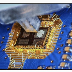
Avicena, a privately held company headquartered in Sunnyvale, CA, is demonstrating the world’s smallest 1Tbps optical transceiver as part its LightBundleTM multi-Tbps chip-to-chip interconnect technology at the SuperComputing Conference (SC23) in Denver, CO. Avicena’s microLED-based LightBundle architecture supports unprecedented throughput, shoreline density and low power, unlocking the performance of processors, memory, and sensors.
Artificial intelligence (AI) is driving an unprecedented surge in demand for compute and memory performance, driven by applications like ChatGPT based on large language models (LLMs). These sophisticated models have an insatiable appetite for computing power and fast access to large amounts of memory, resulting in an urgent and growing demand for much higher density low-power interconnects between Graphics Processing Units (GPUs) and high-bandwidth memory (HBM) modules. Today, HBM modules must be co-packaged with GPUs because the GPU-memory electrical interconnect is limited to just a few millimeters in length. Subsequent HBM generations will require IC shoreline densities in the range of 10Tbps/mm or more. Conventional optical interconnects based on VCSELs or Silicon Photonics (SiPh) promise to extend the interconnect reach but struggle to meet size, bandwidth density, power, latency, operating temperature, and cost requirements. By contrast, Avicena’s microLED-based LightBundle interconnects provide higher bandwidth density, much smaller size, much lower power and latency, and very low costs.
“At Avicena we are excited to showcase the world’s most compact 1Tbps transceiver in the shape of a 3mm x 4mm CMOS ASIC using our patented microLED optical interface,” says Bardia Pezeshki, Founder and CEO of Avicena. “Everyone is talking about SiPh solutions for applications in AI clusters. However, for short reach interconnects with less than 10m reach, we believe that our LED based solution is inherently better suited because the compact size, higher bandwidth density, lower power and latency, and temperature tolerance up to 150°C.”
Avicena’s innovations are supported by key investors including Samsung Catalyst Fund, Cerberus Capital Management, Clear Ventures, and Micron Ventures.
“Optical interconnect technology has the potential to improve chip-to-chip and inter-rack performance,” says Marco Chisari, head of the Samsung Semiconductor Innovation Center. “With a roadmap to multi-Tbps capacity and sub-pJ/bit power efficiency, Avicena’s innovative LightBundle interconnects can enable the next era of AI innovation, paving the way for even more capable models and a wide range of AI applications that will shape the future.”
Share on:


Testimonial
"Advertising in PCB007 Magazine has been a great way to showcase our bare board testers to the right audience. The I-Connect007 team makes the process smooth and professional. We’re proud to be featured in such a trusted publication."
Klaus Koziol - atgSuggested Items
I-Connect007 Editor’s Choice: Five Must-Reads for the Week
10/24/2025 | Andy Shaughnessy, I-Connect007This week, we have quite a bit of international content in this week’s list of must-reads. Nothing happens in a vacuum, including electronics manufacturing and design, and this has been quite an eventful year. How many of us are now tariff experts? I’m certainly not, but that hasn’t stopped me from opining about the situation.
AI Triggers Next Paradigm Shift in PDN
10/23/2025 | Istvan Novak, SamtecArtificial intelligence (AI), together with machine learning (ML), is creating an unprecedented surge of computing and networking infrastructure needs. This, in turn, has dramatically increased the power consumption of computing and networking chips.
PDN Optimization: Balancing Performance and Cost in SoC Designs
10/22/2025 | Zach Caprai. Siemens EDAThis article demonstrates advanced PDN optimization techniques through a real-world case study of AMD’s Versal adaptive SoC platform. Using the VCK190 evaluation kit featuring the Versal AI Core series VC1902 device, I’ll explore how effective PDN design and optimization can help meet demanding technical specifications while addressing essential business goals.
Beyond Design: The Fundamental Structure of Spectral Integrity
10/21/2025 | Barry Olney -- Column: Beyond DesignImpedance can be characterized in both the time and frequency domains. In the time domain, it influences how electromagnetic energy propagates through interconnects, affecting signal integrity and waveform fidelity. In the frequency domain, AC impedance determines how well the network can suppress noise and deliver clean power at a range of frequencies. AC impedance shapes how power rails respond to transient loads.
NOVOSENSE, UAES and Innoscience Advance Power Electronics for New Energy Vehicles
10/20/2025 | PRNewswireThe partnership focuses on developing next-generation intelligent integrated Gallium Nitride (GaN) products. Leveraging their combined expertise, the new devices will deliver more reliable GaN driving and protection features, enabling higher power density and paving the way for wider adoption in automotive systems.