


 Happy’s Tech Talk #44: Memories of the ‘Mystery Systems of the East’
 The Right Approach: Electro-Tek—A Williams Family Legacy, Part 2
 Alpha Insights, Performance by Design: Understanding Heat at the Core of Every Design


ViTrox's Cutting-Edge V510i 3D AOI Wins the 2023 Global Technology Award, Redefining Inspection Excellence
November 23, 2023 | ViTroxEstimated reading time: 2 minutes
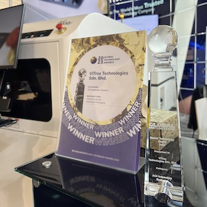
ViTrox, which aims to be the world’s most trusted technology company, is honoured to announce that our latest V510i Advanced 3D Optical Inspection (AOI) Solution for Advanced Packaging has been awarded a 2023 Global Technology Award, in the Inspection - AOI category, from Global SMT & Packaging. The award was announced during the award ceremony at Productronica in Munich, Germany, on November 14, 2023.
With the pioneer integration of Artificial Intelligence (A.I.) technologies and extensive inspection capability, our V510i 3D AOI Solution for Advanced Packaging marks a significant shift in inspection for the semiconductor and SMT industry, especially for highly reflective die and components. One significant breakthrough technology is the Surface Defect Inspection (SDI) algorithm, which enables this V510i 3D AOI solution to offer extensive inspection coverage, including die placement, die coplanarity, die chip-off/crack, die polarity, surface defects on die (such as scratches and contamination), gold pad surfaces, foreign material, and distance measurement. Complemented by the lighting module and motorised z-height, measurements can also be extracted by the Smart Measurement feature, providing CMM-like capabilities.
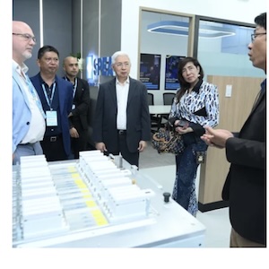
(Group photo of ViTrox and MVTech teams proudly displaying the Global Technology Award 2023 trophy in front of the booth)
By integrating A.I. features in our V510i 3D AOI, users can automate programming and buy-off processes, reducing the need for skilled manual labour and minimising human error risks. Our AI-powered smart programming for AOI provides intelligent and automated programming to minimise human skills dependency and rapidly improve programming time by up to 4 times. In addition, we also offer another A.I. feature – A.I. Assisted Defect Review (also known as A.I. ViTrox Verification Tool Solution) where users can also automate buy-off processes in repair stations. This groundbreaking technology ensures a remarkable accuracy rate of over 90%, offering customers an unrivalled confidence level in the inspection results. On top of our AOI being IPC-CFX-2591 QPL validated, this solution is also SECS/GEM ready.
“With the release of this cutting-edge technology, I am confident that we will help the customer to address their pain points when adapting to Industry 4.0. This award comes as full amazement and honour to us. I would like to take this opportunity to demonstrate my greatest gratitude to the jury for selecting our V510i 3D AOI for Advanced Packaging for this prestigious award. The greatest honour goes to the team who never gives up on innovating the latest technology to bring greater value to fulfil customers' needs and meet their expectations,” said Mr Wee Kah Khim, CEO of Board Inspection and Embedded Solutions (BIE).
Share on:


Testimonial
"We’re proud to call I-Connect007 a trusted partner. Their innovative approach and industry insight made our podcast collaboration a success by connecting us with the right audience and delivering real results."
Julia McCaffrey - NCAB GroupSuggested Items
Merlin PCB Group Invests in 2 CIMS Galaxy 25µ AOI Machines
11/13/2025 | Merlin PCB GroupThe Merlin PCB group has invested in CIMS Galaxy 25µ AOI machines, one for Merlin Flex in Hartlepool and the other for Merlin Circuit Technology in Hawarden.
GenI Generative AOI Programming Debuts: Mycronic Sets a New Standard in AOI Automation
11/10/2025 | MycronicMycronic’s PCB Assembly Solution division announces the launch of GenI™, an industry first solution designed to liberate electronics manufacturers from the complexities of traditional Automated Optical Inspection (AOI) programming.
Learning With Leo: UHDI—The Next Leap in PCB Manufacturing
11/05/2025 | Leo Lambert -- Column: Learning With LeoHigh density interconnect (HDI) technology has been a cornerstone of miniaturized electronics since Hewlett-Packard introduced the first chip-scale implementation in 1982. Over time, HDI processes became central to organic flip-chip packaging in the semiconductor industry. Today, the convergence of IC substrates and system-level PCBs has accelerated the adoption of UHDI.
Koh Young Technology Appoints Jeff Lee as Head of Industrial Solutions Business
11/03/2025 | Koh Young TechnologyKoh Young Technology, the global leader in True 3D measurement-based inspection and metrology solutions, has appointed Jeff Lee as Head of Industrial Solutions Business.
UHDI Fundamentals: UHDI Technology and Automated Inspection
11/03/2025 | Anaya Vardya, American Standard CircuitsFollowing up on the last article on integrating ultra high density interconnect (UHDI) PCB technologies and Quality 5.0, here we will do a deeper dive into the automated inspection component. UHDI applications demand extreme precision, with line/space dimensions below 25 µm and microvias below 30 µm. Automated inspection systems are essential to achieving the defect-free fabrication required at these scales, and legacy automated inspection systems are becoming obsolete and ineffective.