


 The Government Circuit: News on Defense Electronics, Europe, and Sustainability
 American Made Advocacy: Taking the Fight to Capitol Hill
 Defense Speak Interpreted: SWaPing Nanosatellites for Defense Systems
Exploring Cold Milling as an Alternative PCB Component Removal Method
January 24, 2024 | Bob Wettermann, BEST Inc.Estimated reading time: Less than a minute
When a PCB undergoes multiple heat cycles, inherent risks emerge, primarily due to the expansion and contraction of materials. This thermal stress can induce various issues, including delamination, warping, compromised solder joints, and damage to heat-sensitive components like integrated circuits or capacitors.
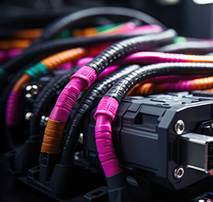
To counter these risks, one approach involves a unique process called "cold milling," designed to mitigate the adverse effects of additional thermal stress. Unlike traditional methods involving direct heat application, this solution utilizes a laser-guided precision mill to remove components. This ESD-safe process includes a vacuum nozzle that simultaneously removes debris during the milling process, ensuring cleanliness.
The genesis of “cold milling” stems from a customer's challenge with removing underfilled BGAs. They encountered issues with underfill leaching into the adjacent solder during reflow, causing solder shorts. By utilizing this cold milling process, we were able to remove the component without applying heat and place a new component in its place resulting in a yield >90% and a successful solution for the customer.
To read this entire article, which appeared in the January 2024 issue of SMT007 Magazine, click here.
Share on:


Suggested Items
HCLTech Announces AI-based Solutions Powered by Intel Core Ultra Processors
10/04/2024 | HCLTechHCLTech, a leading global technology company, will provide advanced AI-driven digital workplace solutions utilizing Intel Core Ultra processors.
KYZEN to Feature Full Line of Metal Cleaning Chemistries at FABTECH
10/01/2024 | KyzenKYZEN, the global leader in innovative environmentally responsible cleaning chemistries, will exhibit at FABTECH 2024, scheduled to take place October 15-17, 2024 at the Orange County Convention Center in Orlando, FL.
Welcome Day: AT&S Trains 21 New Apprentices for the High-tech Industry
09/26/2024 | AT&SNine apprentices started their training at AT&S in 2021. Since then, the Styrian company, one of the world’s leading manufacturers of IC substrates and high-end printed circuit boards, has intensified its apprenticeship training.
Connect the Dots: Designing for Reality—Outer Layer Imaging
09/26/2024 | Matt Stevenson -- Column: Connect the DotsWelcome to the next step in the manufacturing process—the one that gets the chemical engineer in all of us excited. I am referring to outer layer imaging, or how we convert digital designs to physical products. On a recent episode of I-Connect007’s On the Line with… podcast, we explained how the outer layer imaging process maps the design’s unique features onto the board.
Siemens Extends Collaboration with TSMC to Advance Integrated Circuit and Systems Design
09/25/2024 | SiemensSiemens Digital Industries Software today announced it has extended its longstanding collaboration with TSMC through multiple new development projects, product certifications and innovative technology enablement for the foundry’s newest process technologies.