


 Trouble in Your Tank: At 40 GHz, Everything Matters, Part 2
 It’s Only Common Sense: Stop Watching the Headlines and Start Watching the Opportunity
 The Right Approach: The Pros and Cons of PCB Vertical Integration


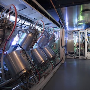
Intel Corp. and United Microelectronics Corporation, a leading global semiconductor foundry, announced that they will collaborate on the development of a 12-nanometer semiconductor process platform to address high-growth markets such as mobile, communication infrastructure and networking. The long-term agreement brings together Intel’s at-scale U.S. manufacturing capacity and UMC’s extensive foundry experience on mature nodes to enable an expanded process portfolio. It also offers global customers greater choice in their sourcing decisions with access to a more geographically diversified and resilient supply chain.
“Taiwan has been a critical part of the Asian and global semiconductor and broader technology ecosystem for decades, and Intel is committed to collaborating with innovative companies in Taiwan, such as UMC, to help better serve global customers,” said Stuart Pann, Intel senior vice president and general manager of Intel Foundry Services (IFS). “Intel’s strategic collaboration with UMC further demonstrates our commitment to delivering technology and manufacturing innovation across the global semiconductor supply chain and is another important step toward our goal of becoming the world’s second-largest foundry by 2030.”
Jason Wang, UMC co-president, said, “Our collaboration with Intel on a U.S.-manufactured 12 nm process with FinFET capabilities is a step forward in advancing our strategy of pursuing cost-efficient capacity expansion and technology node advancement in continuing our commitment to customers. This effort will enable our customers to smoothly migrate to this critical new node, and also benefit from the resiliency of an added Western footprint. We are excited for this strategic collaboration with Intel, which broadens our addressable market and significantly accelerates our development roadmap leveraging the complementary strengths of both companies.”
The 12 nm node will utilize Intel’s U.S. based high-volume manufacturing capacity and experience in FinFET transistor design, offering a strong combination of maturity, performance and power efficiency. The production will markedly benefit from UMC’s decades of process leadership and history of providing customers with Process Design Kit (PDK) and design assistance for effectively providing foundry services. The new process node will be developed and manufactured in Fabs 12, 22 and 32 at Intel’s Ocotillo Technology Fabrication site in Arizona. Leveraging existing equipment in these fabs will significantly reduce upfront investment requirements and optimize utilization.
The two companies will work to satisfy customer demand and cooperate on design enablement to support the 12 nm process by enabling electronic design automation and intellectual properties solutions from ecosystem partners. Production of the 12 nm process is expected to begin in 2027.
Intel has been investing and innovating in the U.S. and globally for more than 55 years, with established or planned manufacturing sites and investments in Oregon, Arizona, New Mexico and Ohio, in addition to Ireland, Germany, Poland, Israel and Malaysia. IFS has made significant progress over the past year, building strong momentum with new customers, including new customers across the Intel 16, Intel 3 and Intel 18A process technologies, and expanding its growing foundry ecosystem. IFS expects to continue its progress this year.
UMC has a more than 40-year history of being a preferred supplier of foundry services to critical applications including automotive, industrial, display and communications. Over the past two decades, UMC has successfully expanded its base across Asia and has continued to lead innovation across mature nodes and specialty foundry services. UMC is a significant supplier to the top 400+ semiconductor customers and has extensive expertise and know-how in supporting customers to reach high yields while maintaining industry-leading foundry utilization.


