


 American Made Advocacy: PCBs in the National Spotlight
 Defense Speak Interpreted: Extreme Financial Disparity in Drones and Missiles
 The Right Approach: The End of an Era—DoD Proposes MIL-PRF-31032 Cancellation


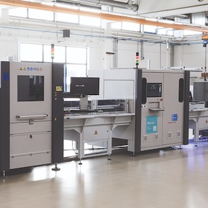
Rehm Thermal Systems is showcasing innovative solutions in vapor phase soldering, coating, and dispensing systems at the IPC APEX EXPO in Anaheim, USA. The IPC APEX EXPO 2024 is the largest electronics manufacturing event in North America, featuring a cutting-edge technological conference, professional training courses by industry experts, and inspiring networking opportunities. Rehm Thermal Systems is presenting the ProtectoXP dispensing system and the CondensoXC vapor phase soldering system at booth 1848 in the Anaheim Convention Center from April 9 to 11, 2024.The Rehm experts on-site are available to answer questions about dispensing various materials for assembly processes, as well as for potting and securing components. At booth 1848, you can witness live demonstrations of the ProtectoXP dispensing system, showcasing its diverse applications and the new integrated 3D height sensor and learn everything about the injection principle in vapor phase soldering with the CondensoXC.
Innovative production line concepts with the ProtectoX series
Smart factory concepts and line integration are key focus areas in the industry. The demands on the new generation of manufacturing systems have grown steadily. Today, it's not just about individual machines but about line solutions, with "turnkey" being the keyword. Whether it's a new or existing process, deep expertise is required to consider all eventualities. If the entire coating process is new to manufacturing, the complexity increases. The integration of a completely new line requires a thorough technological understanding to coordinate and implement the necessary tests and evaluations.
For Rehm Thermal Systems, the conception of a turnkey solution focuses not only on the equipment but especially on the complete dispensing process. This involves determining whether additional sealing, bonding, and dispensing applications should be included in addition to the painting process. Explore the diverse possibilities of our Conformal Coating and Dispensing portfolio with our experts on-site. The systems feature numerous features that simplify the painting process and ensure its success.
A height sensor with Z-position ensures optimal compensation during the dispensing of assemblies that are not planar due to their nature. Since the height must remain constant, automatic height adjustment is essential for a secure process. Another advantage is the 2D programming on 3D objects. Programming is done in 2D, the height sensor scans the adhesive path of the component being dispensed on, and automatically generates the height contour. This automatically creates the appropriate program for this component.
With the ViCON Protecto system software, only a few steps separate the assembly layout from the final coating. Meet our experts on-site and also discover the new integrated 3D height sensor of this coating and dispensing system.
Resource-efficient vapor phase soldering with the Condenso series
In the world of vapor phase soldering systems, vacuum soldering has been a proven technique for decades to significantly reduce air inclusions in solder joints. Rehm has employed a future-proof, sustainable solution from the beginning with the integrated Closed-Loop System for the injected medium Galden® in the vapor phase soldering systems of the Condenso series.
The principle is both efficient and resource efficient. After soldering, the vacuum and/or cooling process begins. Simultaneously, the process gas is suctioned and cleaned. The suction creates a vacuum, ensuring rapid drying of the solder and the process chamber, minimizing losses when ejecting the products.
The suctioned Galden® is filtered and cleaned of impurities using granules. Approximately 99.9% of the medium can be recovered. The cleaned liquid is stored at room temperature in a container and made available for further processes. This eliminates evaporative losses and energy losses. The hermetic isolation of the process chamber (simultaneously vacuum chamber) also eliminates "evaporation loss" during soldering. In addition to minimal maintenance, operating costs are reduced due to lower Galden® consumption.
Innovative M2M communication for board-flow management in SMT assembly lines
The Hermes Standard provides a manufacturer-independent, overarching protocol for Machine-to-Machine (M2M) communication in assembly manufacturing. The goal is to improve or simplify board-flow management, traceability, and electrical wiring across all stations of an SMT line. Modern communication technology and standardized data formats for M2M communication (TCP/IP and XML-based protocol) are extensively utilized. As a next-generation technology, the Hermes Standard is officially recognized and derived from the IPC-SMEMA-9851 standard. In the long term, "The Hermes Standard" is designed to replace the existing SMEMA interface. With IPC recognition, The Hermes Standard Initiative has achieved a significant milestone in the digitization of electronics manufacturing.


