


 Defense Speak Interpreted: Extreme Financial Disparity in Drones and Missiles
 American Made Advocacy: Five Years of Educating, Advocating, and Influencing Legislation and Policy
 The Right Approach: The End of an Era—DoD Proposes MIL-PRF-31032 Cancellation


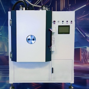
StenTech® Inc., a leading global company specializing in SMT Printing Solutions, will introduce the new StenTech BluPrint™ Chemical Vapor Deposited (CVD) Surface Treatment at the 2024 IPC APEX EXPO. This groundbreaking technology, designed to enhance SMT processes with unparalleled benefits for stencil performance, longevity, and overall assembly quality, will be showcased for the first time in Booth 1608 from April 9-11, 2024 at the Anaheim Convention Center in California.
The relentless drive to shrink components and circuit boards poses challenges in solder paste printing with laser-cut stainless-steel stencils. StenTech BluPrint™ CVD emerges as the premier solution in North America, aligning with the intricate demands of the semiconductor and EMS industry, backed by cutting-edge laser technology advancements.
StenTech BluPrint™ CVD Surface Treatment introduces a revolutionary method of depositing thin films onto a substrate by introducing chemical precursors into a reactor chamber, resulting in a solid material deposit on the surface. The consistency achieved across all areas distinguishes StenTech's CVD from traditional liquid spray processes, providing a resilient, virtually indestructible coating that ensures uniform printing with identical apertures.
Beyond consistent thickness, StenTech BluPrint™ offers exceptional thermal stability, chemical inertness, anti-stiction properties, a refined smooth surface finish, customizable characteristics, and unmatched print quality consistency. The process begins with plasma polishing, followed by the chemical vapor deposition, resulting in a smoother sidewall and enhanced corrosion resistance.
StenTech BluPrint™ stands out with its application at approximately 1000 times less thickness compared to existing alternatives, ranging from 3-5 micrometers versus 3 nanometers. Positioned as the practical choice for coating high-end SMT solder paste stencils, StenTech BluPrint™ promises noticeable enhancements in transfer efficiency, outperforming current nano-coatings, particularly in high-volume builds.
StenTech invites attendees to Booth 1608 at the 2024 IPC APEX EXPO to explore the StenTech BluPrint™ CVD Surface Treatment and experience firsthand its transformative impact on SMT processes.


