


 It’s Only Common Sense: Marketing Isn’t Fluff, It’s Ammunition
 Driving Innovation: Mechanical and Optical Processes During Rigid-flex Production
 The Chemical Connection: Onshoring PCB Production—Daunting but Certainly Possible


Checking In With ICAPE Group
April 3, 2024 | Nolan Johnson, I-Connect007Estimated reading time: 2 minutes
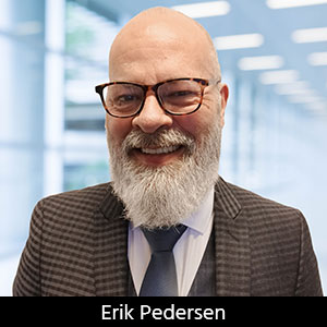
ICAPE Group’s field application engineer Erik Pederson drills down on sustainability, supply chain resiliency, and what value engineering really looks like in this exclusive interview. Founded in 1999, European-based ICAPE Group provides 21 million printed circuit boards and over six million technical parts to manufacturers every month. With 30 PCB manufacturing partners globally and 50 partners providing a wide array of technical parts, ICAPE Group has operations in China, Taiwan, Thailand, South Korea, Vietnam, South Africa, Europe, Mexico, and the United States. The company also focuses on the value proposition for its customers.
Sustainability
Nolan Johnson: How does ICAPE Group incorporate sustainable practices into manufacturing printed circuit boards?
Erik Pederson: There are many things that we do in the process of manufacturing a PCB that focuses on sustainability. PCB fabricators reclaim precious metals from waste and have done so for many years, sending it out to salvage companies that reclaim the metals. Regarding epoxy fiberglass laminate, we can grind it down to small particles that can be used as filler material in things like construction and concrete. As far as the processes themselves, we minimize waste and reclaim materials in as many steps as possible. On the electrolytic copper plating line, when the small copper balls (anodes) are sufficiently depleted, we collect them and send them to salvage for recovery. It is also common to collect router dust from drilling and routing to reclaim especially the gold particles. We reclaim the HASL and precious metals from rinsing during the wet processes. In the etch process, the spent etchant is treated to remove the copper, which is also recovered. This has all been going on for many years, but for someone unfamiliar with the fabrication process, it is important to educate them on all we do to reduce waste.
Johnson: Today, sustainability is not something we only think about during the manufacturing process. PCB fabricators have been focused on environmental sustainability, reducing waste, and maximizing ROI in many ways for decades. Working toward better sustainability really should start long before the board arrives at the PCB shop, correct?
Pederson: That is correct, Nolan. Probably the most important thing we do is to work on sustainability with our customers at the design stage. What are the most (ENIG) and least impactful (OSP) surface treatments to the environment? What is the cost? We also promote the use of halogen-free material. It is my personal belief that customers should pay more attention here. The halogens used to make the fire-retardant materials remain even when you grind down the waste materials. They are harmful to the environment. Today, there are halogen-free materials that have as good a performance as halogen materials, but they cost 20–30% more. But if most PCB makers (and OEMs) would use halogen-free material, the market would drive the price down and they would become more common, addressing a significant environmental issue. One example is NOKIA and Samsung requiring halogen-free material for their PCBs.
To read this entire conversation, which appeared in the March 2024 issue of PCB007 Magazine, click here.
Share on:


Testimonial
"We’re proud to call I-Connect007 a trusted partner. Their innovative approach and industry insight made our podcast collaboration a success by connecting us with the right audience and delivering real results."
Julia McCaffrey - NCAB GroupSuggested Items
High Density Packaging User Group Announces ASKPCB Membership
11/03/2025 | HDP User GroupHigh Density Packaging User Group (HDP) is pleased to announce that the Aoshikang Technology (Hong Kong) Co., Ltd (ASKPCB) has become a member.
TTM Technologies Receives Two Awards from the Global Electronics Association at the 2025 IPC CEMAC Conference
11/03/2025 | Globe NewswireTTM Technologies, Inc. announced that two of its team members received prestigious Asia Steering Committee Outstanding Service Awards from the Global Electronics Association (formerly named IPC connecting global electronics industry) at the 2025 IPC CEMAC Electronics Manufacturing Annual Conference in Shanghai.
PCBAA Names Industry Veteran Dan Weber to Board of Directors
10/31/2025 | PCBAAThe Printed Circuit Board Association of America has added Dan Weber, Executive Vice President and General Counsel at TTM Technologies, to the PCBAA board of directors.
UAE Automotive PCB Research Report 2025: A $971.16 Million Market by 2030
10/31/2025 | Globe NewswireThe UAE Automotive PCB Market was valued at USD 654.07 Million in 2024, and is projected to reach USD 971.16 Million by 2030, rising at a CAGR of 6.80%.
KLA Reports Fiscal Q1 2026 Results
10/31/2025 | PRNewswireKLA Corporation announced financial and operating results for its first quarter of fiscal year 2026, which ended on Sept. 30, 2025, and reported GAAP net income of $1.12 billion and GAAP net income per diluted share of $8.47 on revenues of $3.21 billion.