-

- News
- Books
Featured Books
- pcb007 Magazine
Latest Issues
Current Issue
Engineering Economics
The real cost to manufacture a PCB encompasses everything that goes into making the product: the materials and other value-added supplies, machine and personnel costs, and most importantly, your quality. A hard look at real costs seems wholly appropriate.
Alternate Metallization Processes
Traditional electroless copper and electroless copper immersion gold have been primary PCB plating methods for decades. But alternative plating metals and processes have been introduced over the past few years as miniaturization and advanced packaging continue to develop.
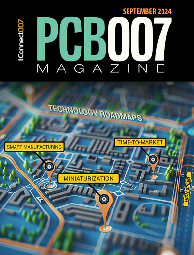
Technology Roadmaps
In this issue of PCB007 Magazine, we discuss technology roadmaps and what they mean for our businesses, providing context to the all-important question: What is my company’s technology roadmap?
- Articles
- Columns
Search Console
- Links
- Media kit
||| MENU - pcb007 Magazine
Silicon Box Selects Piedmont to Host €3.2B Chip Foundry for Italian Expansion
July 2, 2024 | Silicon BoxEstimated reading time: 3 minutes
The co-founders of Silicon Box, CEO Dr. Byung Joon (BJ) Han, Dr. Sehat Sutardja, and Weili Dai, together with the Minister Adolfo Urso, Presidente Alberto Cirio of the Piedmont region, and Mayor Alessandro Canelli of the municipality of Novara announced that Novara in Piedmont will be the site of the company’s new, first-of-a-kind advanced semiconductor packaging and testing foundry. The parties signed a letter of intent outlining their commitment for collaboration related to the site and investment, this morning, at the Ministry of Enterprises and Made in Italy in Rome, subject to the European Commission approval of the planned financial support to be granted by Italy.
The site in Novara and Piedmont was selected from a shortlist of sites and regions in Northern Italy (Nord Italia) through a detailed evaluation process. This effort aimed at ensuring that selection be aligned with the requirements and conditions necessary for the planned facility, and prior commitments agreed between Silicon Box and the Italian government.
“Silicon Box’s advanced packaging facility in Novara is expected to create up to 1,600 highly paid jobs and bring first-of-a-kind advanced semiconductor packaging and testing capabilities to Italy, and to Europe,” said Dr. Byung Joon Han, CEO and cofounder of Silicon Box. “We appreciate the cooperation of all the sites, municipalities and regions that participated in our evaluation process. Every site was carefully reviewed and considered, and each had its own independent merits that reinforced our decision to build in Italy.”
Earlier this year, Silicon Box announced its intention to collaborate with the Italian government to invest up to €3.2B ($3.6B) in Northern Italy, as the site of a state-of-the-art semiconductor assembly and test facility. The facility will help meet critical demand for advanced packaging capacity to enable next generation technologies that Silicon Box anticipates by 2028. The multi-year investment replicates Silicon Box’s flagship foundry in Singapore, which has demonstrated capability and capacity for the world’s most advanced semiconductor packaging solutions, before further expansion into 3D integration and testing. The new integrated production facility is expected to serve as a catalyst for broader ecosystem investments and innovation in Italy, as well as the rest of the European Union.
“We are excited to bring Italy to the forefront of chiplet deployment and the semiconductor industry, through this investment into the world’s most advanced packaging solution. It will enhance competitive strengths in design, artificial intelligence (AI), large language models (LLMs), electronic vehicles (EVs) and automotive, mobile, wearables, smart consumer, edge computing, and material sciences of the Italian ecosystem, and revolutionize Europe’s position in the global [semiconductors] supply chain,” said Dr. Sehat Sutardja, co founder and Chairman of Silicon Box.
“Design and planning for the facility is already underway, with construction to commence pending European Commission approval of planned financial support by the Italian State,” added co-founder, Weili Dai.
Silicon Box’s technology enables advanced chiplet integration (“advanced packaging”), on a large manufacturing format for scale and efficiency. The chiplet concept is an alternative to conventional semiconductor manufacturing, which focused on building entire systems on-chips (SoCs) on silicon wafers, then moving to traditional packaging processes. Chiplets describe manufacture of individual system modalities as standalone “chiplets” on a wafer, then integrating these separate functionalities into a system through advanced packaging, creating a system-in-package (SiPs).
The chiplet concept itself was introduced by Silicon Box co-founder Dr. Sutardja at the International Solid State Circuits Conference (ISSCC) in 2015, where he was plenary speaker. Dr. Han is the inventor of semiconductor packaging solutions fundamental to enable chiplets through advanced packaging. Their long-standing collaboration has been the basis for Silicon Box’s record-breaking progress as a company in the semiconductor manufacturing space, traditionally dominated by a few large companies.
Silicon Box’s Novara factory is planned to begin construction in mid-2025, with initial production expected to begin in 2028.
Suggested Items
CHIPS for America Announces Up to $300M in Funding to Boost U.S. Semiconductor Packaging
11/21/2024 | U.S. Chamber of CommerceThe Biden-Harris Administration announced that the U.S. Department of Commerce (DOC) is entering negotiations to invest up to $300 million in advanced packaging research projects in Georgia, California, and Arizona to accelerate the development of cutting-edge technologies essential to the semiconductor industry.
Advanced Packaging: Preparation is Now
11/20/2024 | Nolan Johnson, SMT007 MagazineA new IPC white paper, “Advanced Packaging to Board Level Integration—Needs and Challenges,” authored by Devan Iyer, chief strategist of advanced packaging, and Matt Kelly, chief technology officer, shares expertise on and advocacy for advanced packaging. In this conversation, they share details from the paper about the complexities of advanced packaging technology and provide additional insight into how next-generation packaging will change how printed circuit boards will be designed, fabricated, and assembled, including final system assembly implications.
Coastal RF Systems Joins StratEdge’s Network as Manufacturer’s Representative for Southern California
10/31/2024 | StratEdgeStratEdge Corporation, a leader in high-performance semiconductor packaging solutions, has appointed Coastal RF Systems as its exclusive Manufacturer's Representative for Southern California.
SEMICON Japan 2024 to Expand Scope with Spotlight on Advanced Design Innovation
10/23/2024 | SEMISEMICON Japan 2024, the largest gathering of leaders from the microelectronics manufacturing supply chain in Japan, will assemble more than 1,000 exhibitors showcasing semiconductor solutions for smart technologies from Dec. 11-13 at Tokyo Big Sight.
Unlock Unmatched Performance for Matched Impedance Devices with StratEdge at IEEE BCICTS 2024
10/22/2024 | StratEdgeStratEdge Corporation, an industry leader in high-frequency and high-power semiconductor packaging, is excited to announce its participation in the IEEE BiCMOS and Compound Semiconductor Integrated Circuits and Technology Symposium (BCICTS).

