


 Standard of Excellence: Building Excellence From the Inside Out
 Powering the Future: Why True Ceramic Circuits Are Not Just ‘Better PCBs’
 Global Sourcing Spotlight: The Global Quality Gap—Why Consistency Wins the Contract


Modern day computing needs, notably AI/machine learning and high-performance computing, along with their subsequent memory and I/O requirements, are fueling an increased demand for semiconductor devices with higher performance, lower power consumption and latency as well as reduced footprint. For decades Moore’s Law was the driving force in achieving ever-favorable PPA (power performance and area) for system-on-chip (SoC) devices. With the slowdown in process node scaling, the industry has turned its attention to alternatives in an effort to regain the past performance trajectory. Advanced packaging schemes have been instrumental in allowing the disaggregation of monolithic chips into smaller functional blocks (chiplets), technology nodes optimized for their given function, cost and performance targets, and then re-assembled at a package level. System-in-package (SiP), 3D-stacking, 2.5D-Interposers, etc. are prime examples of packaging technologies utilized to make up for Moore’s Law scaling issues.
System designers and packaging providers have invented many solutions for reconnecting chiplets in a cost-effective manner where cost can be considered as a weighted average of power consumed, volume occupied, latency or bandwidth limitations. In addition, interconnect density is seeing a steady increase along with reassembled package sizes forecasted to approach 10x reticle in the near future. The ever-evolving packaging schemes have not come without introducing challenges, however. Packaging processes for high-end devices are seeing a migration from conventional flip chip attach, utilizing mass reflow (MR), to more sophisticated techniques such as thermo-compression bonding (TCB). Where pitch scaling goes below 50 µm solder-capped copper pillars utilizing flux for oxide removal introduce further challenges related to flux application and removal.
This webinar will discuss the Kulicke & Soffa (K&S) response to this challenge with the development of an in-situ oxide removal system which has been shown to enable fluxless TCB in the sub-50 µm regime with demonstrated capability down to ~12 µm. The process has been proven to increase yield and process window size for many applications. K&S has productized its proprietary fluxless TCB technology, primarily targeting solder-based fine pitch applications, but there is a natural path for its applicability toward Cu-Cu TCB as well. There is further potential to extend fluxless Cu-to-Cu TCB down to 5 µm pitch or below making it a viable alternative to hybrid bonding. The benefits of Cu-to-Cu TCB are believed to not only be attractive to integrated device manufacturers (IDMs)/foundry companies due to lower costs, but will be especially attractive to subcontractors and OSATs (outsourced semiconductor assembly and test companies) with limited or no front-end level cleanroom capability.
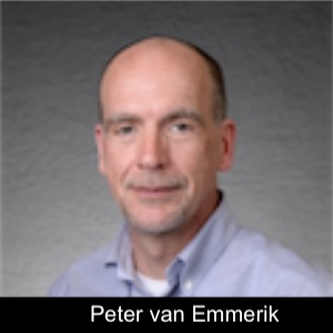
About the Speaker
Peter van Emmerik is a Senior Product Manager at Kulicke & Soffa Industries responsible for the Advanced Packaging Thermo-Compression product portfolio. His current focus is working closely with customers to help them realize their advanced packaging requirements as the industry transitions to larger, fine-pitch die packages and heterogeneous integration of chiplets.
Peter has been with Kulicke & Soffa for almost 20 years and holds both BS and MS degrees in mechanical engineering.
Registration
This webinar is open to industry; advance registration is required (see link below). If you have any questions or need additional information, please contact Masahiro Tsuriya.
August 20, 2024
9:00-10:00 a.m. EDT (Americas)
3:00-4:00 p.m. CEST (Europe)
10:00-11:00 p.m. JST (Japan)
Register for this webinar


