


 Trouble in Your Tank: Understanding Interconnect Defects, Part 1
 It’s Only Common Sense: Marketing Isn’t Fluff, It’s Ammunition
 Driving Innovation: Mechanical and Optical Processes During Rigid-flex Production


Universal Instruments Joins Parent Company Delta to Highlight Comprehensive Semiconductor Solutions at SEMICON Taiwan
August 30, 2024 | Universal InstrumentsEstimated reading time: 1 minute
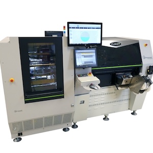
Universal Instruments will join parent company Delta, a global leader in power and thermal management technologies and a world-class provider of industrial automation solutions, on booth S7542 at the SEMICON Taiwan trade show on September 4–6. The booth will feature a seamless integration of semiconductor solutions, including Delta’s Wafer Edge Profile Measurement Machine for front-end processing and Universal’s FuzionSC™ and High-Speed Wafer Feeder back-end multi-die placement solution. Delta will also showcase its Digital-Twin (DlA-Twin) simulation software and adoption of the SEMI E187 cybersecurity practices, surpassing current industry standards.
The Wafer Edge Profile Measurement Machine measures the notch, flat length and edge shape of the ground wafer while also detecting wafer quality and defects. It employs non-destructive AOI optical technology to take these measurements with micro-scale repeatability, which achieves a high throughput of approximately 60-120 wafers per hour. The system supports automated robotic loading/unloading and AGV transport systems, combining diverse functions into a single machine. Delta also offers additional front-end processing solutions including Wafer Edge Grinding, Sorting and IR Pinhole Inspection.
DIATwin is an intelligent design and development tool that can precisely simulate loading points and paths in a virtual environment, enabling the evaluation of production cycle times and reducing the trial-and-error costs in new product introduction. Integrating the DIATwin Virtual Machine Development Platform with front-end equipment to create virtual environments greatly improves efficiency of new product introductions.
The FuzionSC Platform combined with the HSWF is the ultimate solution for challenging multi-die package applications. It’s capable of placing passives and multiple die types in a single cell, eliminating the need to move product between cells and maximizing accuracy and efficiency.
Universal Instruments Vice President of Global Customer Operations and Corporate Marketing, Glenn Farris stated, “The complementary semiconductor solutions we’re able to offer put our customers at the forefront of this fast-moving target. Tying front-end and back-end equipment and processes together, leveraging AI and digital twin technologies to streamline NPI and production, and protecting assets with advanced cybersecurity are all integral advantages.”
Along with visiting the booth, Universal encourages attendees to join a technical presentation by Universal Instruments VP of Global Customer Operations and Corporate Marketing, Glenn Farris. On Friday, September 6 at 11:20 am CST at the HITECH Smart Manufacturing Forum he will present “Accelerating Innovation: Smart Manufacturing for Advanced Semiconductor Packaging”.
Share on:


Testimonial
"Our marketing partnership with I-Connect007 is already delivering. Just a day after our press release went live, we received a direct inquiry about our updated products!"
Rachael Temple - AlltematedSuggested Items
SEMI Reports Worldwide Silicon Wafer Shipments Increase 3% YoY in Q3 2025
11/04/2025 | SEMIThe SEMI Silicon Manufacturers Group (SMG) reported today, in its quarterly analysis of the silicon wafer industry, that worldwide silicon wafer shipments increased 3.1% year-on-year to 3,313 million square inches (MSI) from the 3,214 MSI recorded during the same quarter of 2024.
SEMI Reports Global Silicon Wafer Shipments to Rebound 5.4% in 2025, with New Record Expected by 2028
10/30/2025 | SEMIGlobal shipments of silicon wafers are projected to increase 5.4% in 2025 to 12,824 million square inches (MSI) followed by steady growth through 2028 when the market is expected to reach a new industry record of 15,485 MSI, SEMI reported in its annual silicon shipment forecast.
SEMI Reports Global Silicon Wafer Shipments to Rebound 5.4% in 2025, with New Record Expected by 2028
10/29/2025 | SEMIGlobal shipments of silicon wafers are projected to increase 5.4% in 2025 to 12,824 million square inches (MSI) followed by steady growth through 2028 when the market is expected to reach a new industry record of 15,485 MSI, SEMI reported today in its annual silicon shipment forecast.
Advanced Semiconductor Packaging Market Sees Rising Adoption Across Automotive and Industrial Sectors
10/14/2025 | openPRThe semiconductor packaging market size is estimated to reach at a CAGR of 7.2% during the forecast period (2024-2031).
Too Important to Ignore: Unpacking Advanced Packaging for AI Semiconductor – Report Summary
09/16/2025 | FuturumAdvanced packaging is becoming the cornerstone of AI semiconductor scaling, with 2.5D/3D integration, CoWoS, CPO, CoPoS, and SoW-X set to drive major gains in performance, bandwidth, and efficiency through the 2020s.