-

- News
- Books
Featured Books
- smt007 Magazine
Latest Issues
Current Issue
What's Your Sweet Spot?
Are you in a niche that’s growing or shrinking? Is it time to reassess and refocus? We spotlight companies thriving by redefining or reinforcing their niche. What are their insights?

Moving Forward With Confidence
In this issue, we focus on sales and quoting, workforce training, new IPC leadership in the U.S. and Canada, the effects of tariffs, CFX standards, and much more—all designed to provide perspective as you move through the cloud bank of today's shifting economic market.

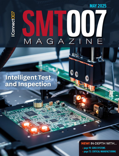
Intelligent Test and Inspection
Are you ready to explore the cutting-edge advancements shaping the electronics manufacturing industry? The May 2025 issue of SMT007 Magazine is packed with insights, innovations, and expert perspectives that you won’t want to miss.
- Articles
- Columns
- Links
- Media kit
||| MENU - smt007 Magazine
Partial HDI: A Complete Solution
October 10, 2024 | I-Connect007 Editorial TeamEstimated reading time: 3 minutes
We recently spoke with IPC instructor Kris Moyer about partial HDI, a process that’s recently been growing in popularity. Partial HDI allows designers to escape route out from tight-pitch BGAs on one layer, where a mechanically drilled plated through-hole is not an option, while avoiding the complexity and expense of sequential lamination cycles.
As Kris explains, this process doesn’t add much to the cost, and it’s fairly straightforward. But there are some competing signal integrity and fabrication requirements to contend with. We asked Kris to walk us through this process.
Andy Shaughnessy: We’ve been talking recently about partial HDI. You’ve been teaching this in your IPC classes. Tell us about it.
Kris Moyer: The BGAs are the most problematic as far as tight pitch, along with the column grid array (CGA), and the land grid array (LGA). All these packages have been going to smaller pitches. When they first came out, we were at 1.27 mm pitch, and you could easily get a mechanically drilled plated through-hole via between the lands. But as you start getting below that pitch to 0.5 mm, 0.4 mm, and smaller, you are not able to place a mechanically drilled plated through-hole in there and still meet the IPC design and producibility requirements. You also need to go to very thin coppers to etch the feature geometries that small. We call this partial HDI, but many companies call it hybrid construction. Fortunately, we can now implement some HDI technology in one lamination cycle without going through full sequential lamination, which is a big advantage.
Shaughnessy: I imagine that there are some trade-offs when we mix technologies like this.
Moyer: Yes. The problem is, it's not just that the pitch is smaller; the size of the land is also smaller, so the spacing between the lands is smaller. In traditional boards, we know how to work with half-ounce copper, or 1-ounce copper. But now we're in quarter-ounce, eighth-ounce, 20-micron, 15-micron, or 5-micron copper thicknesses to get the etching that fine. With a 0.5 millimeter pitch BGA, we're talking about 3 or maybe 2 mils of copper-to-copper between the lands.
You can't etch that out of traditional 1-ounce copper. With these hybrid designs, you can build up all the inner layers with standard 1-ounce copper, but on the outer layer where these BGAs are being attached, you will have to go to very thin coppers and doing some laser-drill microvia technology to get a via feature sufficiently small enough that gets between the pads to get down to that first layer from the solder pads.
Marcy LaRont: You don’t have to do 2-4-2 buildup boards? Is that what we're talking about here?
Moyer: That’s right. The 2-4-2 is full HDI with sequential lamination. The number 4 in 2-4-2 means that you build four layers using standard multilayer fabrication. Then on each of the two sides, the top and the bottom, you add two HDI layers sequentially. With partial HDI, we only need one HDI layer on that one surface. You can build it in one lamination cycle because you only have to laser drill that first outermost layer. But you will need a thin layer to meet the aspect ratio requirements of microvias. You might not necessarily have a reinforcement layer. That's one of the issues that we have with HDI. Often, to get those very thin dielectrics—the 1-mil dielectric layers that we do with HDI layers—we're basically doing resin-coated coppers without any reinforcement material.
To continue reading this article, which appeared in the October 2024 issue of Design007 Magazine, click here.
Suggested Items
The Death of the Microsection
06/26/2025 | Bob Neves, Reliability Assessment Solutions, Inc.I got my start out of college grinding and polishing PCB microsections. My thumbs are a bit arthritic today because of the experience (microsection grinders know what I mean). Back then, via structures were rather large, and getting to the center in six steps of grinding and polishing was easy compared to what my team has been doing recently at the lab.
Day 2: More Cutting-edge Insights at the EIPC Summer Conference
06/18/2025 | Pete Starkey, I-Connect007The European Institute for the PCB Community (EIPC) summer conference took place this year in Edinburgh, Scotland, June 3-4. This is the third of three articles on the conference. The other two cover Day 1’s sessions and the opening keynote speech. Below is a recap of the second day’s sessions.
American Standard Circuits to Exhibit at IMS 2025
06/12/2025 | American Standard CircuitsAnaya Vardya, President and CEO of American Standard Circuits & ASC Sunstone Circuits, announced that his companies will exhibit at the IEEE International Microwave Symposium (IMS 2025), taking place June 15-20, 2025, at San Francisco’s Moscone Center.
UHDI Fundamentals: UHDI Drives Unique IoT Innovation—Smart Homes
06/03/2025 | Anaya Vardya, American Standard CircuitsThe combination of UHDI's high-bandwidth capabilities and IoT's real-time data processing can lead to more efficient, immersive, and smarter IoT systems. This convergence of two revolutionary technologies is enabling quantum advancements in some very “unconventional” applications.
Choosing the Right Strategic Path
04/29/2025 | Marcy LaRont, PCB007 MagazineTom Yang, CEO of CEE PCB, discusses the current economic challenges, noting reduced purchasing power post-pandemic. He highlights the growing demand for HDI in consumer electronics due to AI growth. Tom also expresses concerns about tariffs under the new U.S. administration, prompting CEE to diversify production locations, including new plants in Southeast Asia. He emphasizes the need for PCB manufacturers to adapt strategically amidst rising costs and fierce competition, particularly for mid-sized shops facing unique challenges in the industry.


