


 Trouble in Your Tank: Understanding Interconnect Defects, Part 1
 It’s Only Common Sense: Marketing Isn’t Fluff, It’s Ammunition
 Driving Innovation: Mechanical and Optical Processes During Rigid-flex Production


Back to School With Jonathan Studinka
October 16, 2024 | Andy Shaughnessy, Design007 MagazineEstimated reading time: 3 minutes
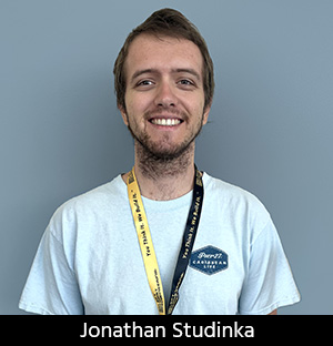
At the Anaheim Electronics & Manufacturing Show, I spoke with Jonathan Studinka, a student in John Watson’s PCB design class at Palomar College. In this interview, Jonathan shares his experience, highlighting how John’s class has broadened his understanding of PCBs and sparked his interest in mechatronics. Despite having no prior electronics training, Jonathan says he finds the coursework manageable by taking it step by step.
Andy Shaughnessy: Jonathan, tell us about your PCB design class at Palomar College.
Jonathan Studinka: It’s opened my eyes to many things about PCBs and the world we live in. The device recording this conversation has a PCB in it, so without that PCB, this interview couldn't happen. I wanted to go to the mechanical side at first. But after taking John Watson’s class, I want to look more into mechatronics, combining mechanical and electrical.
Shaughnessy: You mentioned that you have a background in AutoCAD, correct?
Studinka: Yes, I've learned AutoCAD. At my old company, we built water filtration systems for municipalities around San Diego County, and I helped them design a frame for a mixer that would sit in a tank holding up to 10 million gallons.
Shaughnessy: That's pretty cool. What led you to take Watson’s class?
Studinka: Basically, I was just seeing what was out there. I want to do something hands-on, building something from nothing.
Shaughnessy: How far along are you in the coursework?
Studinka: We're six weeks in. It's a very overwhelming thing when you haven't had a background in PCB, not having touched anything about it before. So, I eat the elephant a few bites at a time.
Shaughnessy: Did you have any prior electronics training?
Studinka: No, no electronics training at all. I thought I would go into construction work, but quickly decided that was not a path for me. We had a construction class in my high school. I realized I didn’t want to go down that path.
Shaughnessy: Well, Watson certainly has a jobs pipeline. He says companies ask him for candidate referrals every day.
Studinka: That would be amazing to go from a class right into a job.
Shaughnessy: Since you already have AutoCAD experience, you could be the part-time mechanical guy instead of having to call the mechanical guy.
Studinka: I think it would be cool to wear multiple hats.
Shaughnessy: Would you recommend this class?
Studinka: I would, absolutely. Give it a shot; you don't know until you try, even if you feel like you're in over your head. John takes you through every single step you need to know. I often think that if I do this and this, what will happen to my design? We're just finalizing the schematic, and even in our lab, I was playing around with different pins and this and that, seeing what it would do. I actually was able to fix a few issues just by playing around and seeing what could happen.
Shaughnessy: It is an art. Some people say it's also like a puzzle. Do you like to do puzzles?
Studinka: Yes, it is like a big jigsaw puzzle where the shapes do not always fit together properly, but they go next to each other.
Shaughnessy: That's a good way to look at it. Any final thoughts?
Studinka: No, just get into PCB design, and you can start with this John’s class at Palomar College.
Shaughnessy: Thank you, Jonathan. Glad to see young people coming into PCB design again.
Studinka: Thank you for the opportunity.
Share on:


Testimonial
"Your magazines are a great platform for people to exchange knowledge. Thank you for the work that you do."
Simon Khesin - Schmoll MaschinenSuggested Items
Aismalibar, Technosystem Showcase Next-Generation PCB Solutions at productronica 2025
11/05/2025 | AismalibarBENMAYOR S.A., parent company of Aismalibar and Technosystem, will present its latest innovations in thermal management materials and PCB automation systems at Productronica 2025, the world’s leading trade fair for electronics development and production.
Ventec to Exhibit Latest Materials and Machinery for Cutting-edge PCB Production at productronica 2025
11/05/2025 | Ventec International GroupVentec International Group will present advanced materials at Productronica 2025 in Munich, ushering in the ‘Glass Free Revolution’ with the latest and pro-bond & thermal-bond bondply materials.
Target Condition: Distribution of Power—Denounce the Ounce
11/05/2025 | Kelly Dack -- Column: Target ConditionHave you ever wondered why the PCB design segment uses ounces to describe copper thickness? There’s a story behind all of this—a story that’s old, dusty, and more than a little absurd. (Note that I didn’t add “Like many of us.”) Legend has it that back in the days of copper tinkers and roofing tradesmen, the standard was set when a craftsman hammered out a sheet of copper until it weighed one ounce, when its area conveniently matched the square of the king’s foot.
High Density Packaging User Group Announces ASKPCB Membership
11/03/2025 | HDP User GroupHigh Density Packaging User Group (HDP) is pleased to announce that the Aoshikang Technology (Hong Kong) Co., Ltd (ASKPCB) has become a member.
TTM Technologies Receives Two Awards from the Global Electronics Association at the 2025 IPC CEMAC Conference
11/03/2025 | Globe NewswireTTM Technologies, Inc. announced that two of its team members received prestigious Asia Steering Committee Outstanding Service Awards from the Global Electronics Association (formerly named IPC connecting global electronics industry) at the 2025 IPC CEMAC Electronics Manufacturing Annual Conference in Shanghai.