-

- News
- Books
Featured Books
- smt007 Magazine
Latest Issues
Current Issue
The Path Ahead
What are you paying the most attention to as we enter 2025? Find out what we learned when we asked that question. Join us as we explore five main themes in the new year.

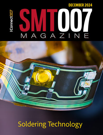
Soldering Technologies
Soldering is the heartbeat of assembly, and new developments are taking place to match the rest of the innovation in electronics. There are tried-and-true technologies for soldering. But new challenges in packaging, materials, and sustainability may be putting this key step in flux.

The Rise of Data
Analytics is a given in this industry, but the threshold is changing. If you think you're too small to invest in analytics, you may need to reconsider. So how do you do analytics better? What are the new tools, and how do you get started?
- Articles
- Columns
Search Console
- Links
- Media kit
||| MENU - smt007 Magazine
Estimated reading time: 5 minutes
Global PCB Connections: Mission Critical—Communication Between PCB Designers and Fabricators
In this, my first column, I discuss the critical importance of communications between the PCB designer and the PCB fabrication engineer. I’ll explore why clear communication is so important, highlight the differences between standard and CTQ items, and outline the key issues that must be agreed upon to achieve success in PCB manufacturing.
As a PCB field applications engineer, I’ve seen the success of countless projects hinge on one simple, yet often overlooked aspect: communication. The relationship between a PCB designer and a fabricator should be seamless, but too often, miscommunications cause costly delays, redesigns, or even complete failures in product development. To prevent this, it’s vital to distinguish between standard items and critical-to-quality (CTQ) elements, ensuring that both sides are aligned from the very beginning.
PCB designers are experts in creativity and engineering, constantly pushing the boundaries of what’s possible in the electronics world. Fabricators, on the other hand, are specialists in turning these designs into physical, manufacturable products. While both sides share the common goal of producing a functional, reliable PCB, they approach the process from different perspectives.
Designers focus on the electrical performance and functionality of the board. They prioritize signal integrity, impedance matching, and ensuring the design meets the specifications of the end product. Fabricators, however, prioritize manufacturability, yield, and ensuring the board can be produced consistently, within budget, and on time. Without clear communication, a perfectly designed board might be impossible to fabricate, or a manufacturable design might compromise the performance the designer intended.
The crux of the problem often lies in the failure to differentiate between what’s standard and what’s critical. Misunderstanding or overlooking these distinctions can lead to manufacturing issues or, worse, field failures. Designers and fabricators must communicate early and often, ensuring they are on the same page throughout the entire process.
Differentiating between standard items and critical-to-quality items: When it comes to PCB design and fabrication, not every detail carries the same weight. Certain aspects of the design are considered standard things that are routine in the manufacturing process and can typically be managed with minimal oversight. These include basic dimensions, typical materials, standard drill sizes, and typical tolerances. These items don’t require significant discussion unless something unique is requested.
However, CTQ items are the components or processes that directly impact the performance, reliability, or manufacturability of the PCB. These elements must be explicitly defined, discussed, and agreed upon by both the designer and the fabricator. They can include things like:
- Trace width and spacing tolerances: Even minor deviations here can cause signal integrity issues, making it essential for both parties to agree on what is acceptable.
- Via and hole sizes: Especially with advanced boards (HDI, flex, etc.), these must be within very tight tolerances to ensure the board performs as expected.
- Material selection: The choice of materials affects everything from thermal performance to signal propagation. Designers often select materials based on performance characteristics, but fabricators need to ensure these materials can be sourced, processed, and managed appropriately.
- Stackup and impedance control: Precise layer stacking and controlled impedance are crucial for high-speed designs, and any misalignment in understanding here can lead to major functional failures.
- Solder mask clearance: Misalignment of solder mask openings can lead to solder bridges, especially in fine-pitch components.
The key is understanding which elements fall under "business as usual" for the fabricator and which require close attention and precision. While it’s easy for a designer to assume that everything is critical, differentiating between the two helps streamline communication and prevents unnecessary delays.
The most successful PCB projects are those where designers engage with fabricators early in the process. Too often, I’ve seen designers hand off their completed designs, expecting a smooth fabrication process, only to be met with a list of issues that force them back to the drawing board. Early engagement can prevent this.
By involving the fabricator during the design stage, designers can get valuable feedback on the manufacturability of their designs. This is especially important for CTQ items. Fabricators can suggest alternative materials, processes, or design tweaks to save time and cost without compromising the board’s functionality.
For example, if a designer specifies a particular laminate material that’s difficult or expensive to source, the fabricator might recommend an alternative with similar performance characteristics but better availability. Or, if the design includes vias that are difficult to plate or drill, the fabricator can suggest changes to make the process easier without affecting the board’s performance.
For a smooth and successful handoff between designer and fabricator, there are several key issues that both sides must agree upon:
- Stackup design: Both parties need to agree on the layer structure, including the materials used, dielectric thicknesses, and copper weights. This is especially critical for controlled impedance designs.
- Material selection: As mentioned earlier, the material affects many aspects of performance and manufacturability. Ensure that the chosen materials are readily available and can be processed by the fabricator.
- Impedance control requirements: Both the designer and the fabricator need to agree on the impedance tolerances and the test methods used to verify them.
- Design rule checks (DRC) and constraints: The designer should share any design rule constraints with the fabricator, ensuring that they are achievable and practical in the manufacturing process.
- Panelization: Fabricators often have specific requirements for how boards are panelized for efficient production. Early agreement on panelization helps ensure manufacturability and yield.
- Plating and Finish: Agreement on the type of finish (e.g., ENIG, OSP, HASL) and plating requirements is critical, as these can impact both the cost and the performance of the board.
- Tolerances and drill sizes: It’s important to agree on acceptable tolerances for trace widths, via sizes, and hole drilling. Fabricators have different capabilities, and the designer needs to understand what’s feasible.
- Test and inspection requirements: Whether it’s electrical testing, visual inspection, or automated optical inspection (AOI), both sides need to agree on how the boards will be tested and what criteria must be met.
- Delivery and lead times: Misaligned expectations on delivery timelines can cause project delays. Both parties should agree on realistic lead times based on the complexity of the design and any special materials or processes involved.
At the heart of any successful PCB project is collaboration. The designer’s vision must be met by the fabricator’s ability to produce a reliable, manufacturable product. Differentiating between standard items and critical-to-quality elements helps focus discussions on the areas that matter most, preventing miscommunication and costly mistakes.
Ultimately, both designers and fabricators must recognize that they are working toward the same goal. Open, early, and clear communication ensures that when the final board comes off the production line, it not only meets design specifications but also is manufacturable at scale and on time. Until next time, let’s stay connected.
Jerome Larez is a field application engineer and technical sales director at CEE PCB.
More Columns from Global PCB Connections
Global PCB Connections: Following DFM Rules Leads to Better BoardsGlobal PCB Connections: A Technical Overview of Long-flex Printed Circuit Boards


