


 Beyond the Board: Early Engagement Means Faster Prototyping for Defense Programs
 Defense Speak Interpreted: The Autonomous Plane Battle—Skyborg Vs. Loyal Wingman
 American Made Advocacy: Congress Back from Break With Work To Do


One Partial HDI Technique: mSAP
November 5, 2024 | Andy Shaughnessy, Design007 MagazineEstimated reading time: 2 minutes
Partial HDI has shown itself to be very useful, allowing designers to escape route tight-pitch BGAs without moving to full HDI and the required sequential lamination. It’s almost the best of both worlds.
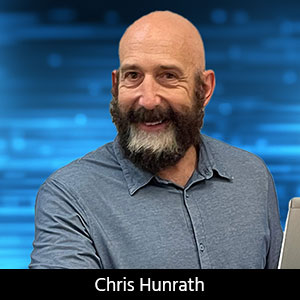
Chris Hunrath, vice president of technology at Insulectro, believes that mSAP just might be the trick for designers considering partial HDI. As Chris explains, the materials and equipment required for the mSAP process are easily available, and the process is well established. This could be a great option for designers working with BGAs that have a pitch of 0.5 mm or less.
Andy Shaughnessy: Chris, why would somebody choose to move to partial HDI? When does that process make sense, and when is mSAP the answer?
Chris Hunrath: It’s all about BGA pitch, microvia location, and circuit routing. I've not heard anyone call it partial HDI, but I like that expression because that explains it just right: the rest of that layer or the board might be more, let's say, conventional. But you neck down the traces to be able to do your fan-out. One of the things I've learned in the past couple of years from designers is that it's okay to make the trace narrower—you won’t degrade the signal integrity as long as that neck-down area is a short length. You can get your routing and still have some registration budget where you won't risk having defects like shorts and whatnot.
First, there’s a lot of what we call “head trash” about exactly what mSAP is. It's also really important to remember that pattern plating, which is done in North American PCB shops every day, is a semi-additive process. We're just taking it to the next level with mSAP. A lot of things are converging right now. You have the finer-pitched BGA packages that are being developed for multiple markets. That's another thing. It's one thing to have lots of room, but if the component is made for multiple markets, you're stuck with that pitch. You just can't go to a bigger pitch.
Another point is that exposure units keep getting better and more capable. If your board shop has a direct imaging machine, you likely already have that 25-micron capability. Some of the materials have come together as well, and we supply those materials.
To read this entire conversation, which appeared in the October 2024 issue of Design007 Magazine, click here.
Share on:


Testimonial
"Your magazines are a great platform for people to exchange knowledge. Thank you for the work that you do."
Simon Khesin - Schmoll MaschinenSuggested Items
MKS’ Atotech Showcases Next-gen PCB and Substrate Manufacturing Solutions at CPCA Plus 2025
10/24/2025 | MKS Inc.MKS Inc., a global provider of enabling technologies that transform our world, announced its participation in CPCA Plus Show 2025, taking place October 28 – 30 at Shenzhen International Convention and Exhibition Center.
Global Electronics Association Releases Fall Schedule of Instructor-led Courses
10/20/2025 | Corey Lynn, Global Electronics AssociationWhether you’re looking to enhance your PCB design skills, explore advanced packaging technologies, or deepen your understanding of reliability, these Global Electronics Association courses deliver high-impact learning from the best in the industry. Here are a few starting this week.
Episode 6 of Ultra HDI Podcast Series Explores Copper-filled Microvias in Advanced PCB Design and Fabrication
10/15/2025 | I-Connect007I-Connect007 has released Episode 6 of its acclaimed On the Line with... American Standard Circuits: Ultra High Density Interconnect (UHDI) podcast series. In this episode, “Copper Filling of Vias,” host Nolan Johnson once again welcomes John Johnson, Director of Quality and Advanced Technology at American Standard Circuits, for a deep dive into the pros and cons of copper plating microvias—from both the fabricator’s and designer’s perspectives.
Interposers, Substrates, and Advanced Manufacturing
10/13/2025 | Marcy LaRont, I-Connect007I attend a lot of industry trade shows and conferences. Lately, during conversations with technologists, I’ve noticed that there is some confusion about what exactly constitutes an interposer. One question I hear every so often is, “Are all interposers substrates?” The short answer to that question is no. But some interposers are, in fact, full substrates.
I-Connect007 Editor’s Choice: Five Must-Reads for the Week
10/10/2025 | Nolan Johnson, I-Connect007I-Connect007 has a new monthly digest newsletter, the Advanced Electronic Packaging Digest, and as I was scanning our advanced packaging newsfeeds this week, I came across a primer from tokenring.ai (republished through station WRAL, Raleigh, North Carolina), which I found quite useful. Whether you’re a designer, fabricator, or assembler, the package schemes being developed will change how you work, so be sure to keep your eye on the technological horizon and subscribe to the monthly Advanced Electronic Packaging Digest.