


 Dan's Biz Bookshelf: 'Move Your Bus'
 Driving Innovation: Direct Imaging vs. Conventional Exposure
 It’s Only Common Sense: Selling to Today's Generation of Buyers


Cadence Unveils Arm-Based System Chiplet
November 20, 2024 | Cadence Design SystemsEstimated reading time: 2 minutes
Cadence has announced a groundbreaking achievement with the development and successful tapeout of its first Arm-based system chiplet. This innovation marks a pivotal advancement in chiplet technology, showcasing Cadence's commitment to driving industry-leading solutions through its chiplet architecture and framework.
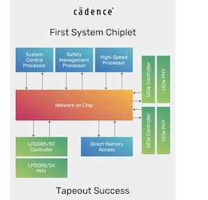
The First System Chiplet
In a significant leap forward, Cadence has successfully prototyped, designed, and taped out the industry's first system chiplet. This chiplet integrates processors, system IP, and memory IP within a single package, interconnected through the Universal Chiplet Interconnect Express™(UCIe™) standard interface. Developed with Arm, the chiplet complies with Arm's Chiplet System Architecture (CSA), a standard that ensures interoperability and speeds time-to-market for chiplets.
A system chiplet includes functionality to manage the resources and functionality of the overall multi-chiplet SoC. Featuring components such as a system processor, safety management processor, Cadence controllers, and Cadence PHY IP for LPDDR5 and UCIe, the chiplet is a testament to Cadence's innovation. Using Cadence Janus NoC technology, the chiplet accommodates up to 64GB/s peak bandwidth for UCIe IP and 32GB/s peak memory bandwidth for LPDDR5 IP.
Advancing the Chiplet Ecosystem with Arm
In March 2024, Cadence and Arm formalized their longstanding collaboration to deliver a chiplet-based reference design and a cutting-edge software development platform. This partnership combines Cadence's robust IP and EDA solutions with Arm's state-of-the-art IP technologies, significantly reducing design complexity and accelerating time-to-market for customers. The alliance sets the stage for further advancements, offering customers a comprehensive development platform for unprecedented performance and efficiency.
The central strategy for this collaboration is investing in the Arm CSA, enabling greater component reuse between suppliers. Cadence is an active contributor to the CSA and is developing chiplets that comply with this standard. These standards allow scale and faster time-to-market for chiplets, including Arm Compute Subsystems (CSS) and the Cadence system chiplet.
Advanced IP Technology Innovations
Capitalizing on decades of expertise in IP and subsystem design, the Silicon Solutions Group delivers high-value solutions that address customer challenges. Abstracting functionality into chiplet IP empowers customers to bring innovations to market more quickly. Cadence's mastery of advanced packaging and interconnect technologies enables scalable, high-performance solutions that enhance efficiency and drive technological progress.
Transforming Industries with Chiplet Technology
The shift from monolithic SoCs to chiplet-based designs is driven by the need for enhanced design efficiency, faster platform refresh cycles, and optimized power, performance, and area (PPA) metrics. Chiplets enable a multi-foundry business model, integrating cross-foundry process technologies within the same package. As technology density scaling slows, chiplets become essential in overcoming Moore's Law limits and process reticle constraints. New packaging and interconnect solutions, including 2.5D and 3D packaging and die-to-die interfaces like UCIe, support this transformative approach, offering customers a path to accelerated innovation and market readiness.
Conclusion
Cadence's pioneering work in chiplet technology represents a significant advance in the semiconductor industry. Cadence is setting new benchmarks for efficiency, scalability, and performance through innovative architectures, robust IP, and strategic partnerships. These developments meet the evolving demands of the high-performance computing, automotive, and data center industries and empower customers to overcome design challenges and accelerate their time to market. Cadence remains committed to pushing the boundaries of technology, shaping the future of the chiplet ecosystem.
Share on:


Suggested Items
Chiplets and the Like are Redefining Microelectronics
06/25/2025 | productronicaThe performance of modern AI and high-performance computing applications can only be achieved with high-performance semiconductor technology.
Cadence, AVCC to Advance Physical AI Innovations for Autonomous Vehicles
05/12/2025 | Cadence Design SystemsCadence has joined the Autonomous Vehicle Computing Consortium (AVCC), marking a significant step forward in Cadence's commitment to advancing autonomous vehicle technology for the physical AI era by working with industry leaders to define high-performance computing (HPC) and safety solutions for next-generation autonomous vehicle systems.
SEMI 3D & Systems Summit to Spotlight Trends in Hybrid Bonding, Chiplet Architecture and Geopolitical Dynamics
05/01/2025 | SEMILeading experts in 3D integration and systems for semiconductor manufacturing applications will gather at the annual SEMI 3D & Systems Summit, June 25-27, 2025, in Dresden.
Keysight EDA, Intel Foundry Collaborate on EMIB-T Silicon Bridge Technology for Next-Generation AI and Data Center Solutions
04/30/2025 | BUSINESS WIREKeysight Technologies, Inc. announced a collaboration with Intel Foundry to support Embedded Multi-die Interconnect Bridge-T (EMIB-T) technology, a cutting-edge innovation aimed at improving high-performance packaging solutions for artificial intelligence (AI) and data center markets in addition to the support of Intel 18A process node.
Global Chiplets Market to Grow at 41.9% CAGR from 2024 to 2029
03/20/2025 | PRNewswireAccording to the latest study from BCC Research, "Global Chiplets Market" will reach $42.8 billion by the end of 2029, growing at a CAGR of 41.9% from 2024 to 2029.