


 American Made Advocacy: Smart Policies Can Ensure AI Data Centers Are Secure
 Beyond the Board: Early Engagement Means Faster Prototyping for Defense Programs
 Defense Speak Interpreted: The Autonomous Plane Battle—Skyborg Vs. Loyal Wingman


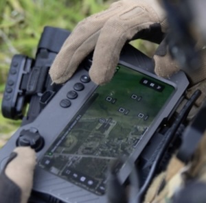
IPC Announces New Training Course: PCB Design for Military & Aerospace Applications
December 23, 2024 | IPCEstimated reading time: Less than a minute
IPC announced the launch of a new training course: PCB Design for Military & Aerospace Applications.
This six-week program, delivered through a combination of live webinars, on-demand sessions, and interactive exercises, will address the unique challenges associated with designing PCBs for military and aerospace applications.
Key Learning Objectives:
- Understand the effects of vibration, shock, radiation, altitude, and extended temperature ranges on PCB design.
- Learn how to design for manufacturability, assembly, and testing in high-reliability applications.
- Master the documentation and manufacturing file generation requirements for military and aerospace projects.
- Taught by an IPC-certified industry expert with over 25 years of experience, this course is designed for designers, engineers, technicians, and anyone involved in the PCB design process for military and aerospace applications.
Prerequisites:
- Completion of IPC’s PCB Fundamentals courses (I and II)
- OR familiarity with schematic symbol creation, schematic generation, documentation, and dimensioning for standard rigid printed boards.
Course Dates:
- January 27, 2025 – March 5, 2025
- Mondays and Wednesdays, 11:00 AM – 1:00 PM CST
Visit IPC website for more information.
Share on:


Testimonial
"Your magazines are a great platform for people to exchange knowledge. Thank you for the work that you do."
Simon Khesin - Schmoll MaschinenSuggested Items
Aircraft Wire and Cable Market to surpass USD 3.2 Billion by 2034
10/30/2025 | Global Market Insights Inc.The global aircraft wire and cable market was valued at USD 1.8 billion in 2024 and is estimated to grow at a CAGR of 5.9% to reach USD 3.2 billion by 2034, according to recent report by Global Market Insights Inc.
The Training Connection Continues to Grow with Addition of Veteran IPC Trainer Bill Graver
10/30/2025 | The Training Connection LLCThe Training Connection, LLC (TTC-LLC), a premier provider of test engineering and development training, is proud to announce the addition of Bill Graver to its growing team of industry experts. A respected professional with more than 35 years in electronics manufacturing, Bill joins as an IPC Master Trainer, bringing a wealth of hands-on experience in PCB testing, failure analysis, and process improvement.
I-Connect007 Welcomes New Columnist: Leo Lambert, EPTAC
10/30/2025 | I-Connect007I-Connect007 is excited to announce a column by Leo Lambert, an industry veteran with 40 years of experience, an award winner, and technical director at EPTAC. This column, Learning With Leo, will explore the evolution and related challenges of electronics product assembly, especially as it relates to training.
On the Line With… Ultra HDI Podcast—Episode 7: “Solder Mask: Beyond the Traces,” Now Available
10/31/2025 | I-Connect007I-Connect007 is excited to announce the release of the seventh episode of its 12-part podcast series, On the Line With… American Standard Circuits: Ultra HDI. In this episode, “Solder Mask: Beyond the Traces,” host Nolan Johnson sits down with John Johnson, Director of Quality and Advanced Technology at American Standard Circuits, to explore the essential role that solder mask plays in the Ultra HDI (UHDI) manufacturing process.
AI Triggers Next Paradigm Shift in PDN
10/23/2025 | Istvan Novak, SamtecArtificial intelligence (AI), together with machine learning (ML), is creating an unprecedented surge of computing and networking infrastructure needs. This, in turn, has dramatically increased the power consumption of computing and networking chips.
Copyright © I-Connect007 | IPC Publishing Group Inc. All rights reserved.
Log in