





















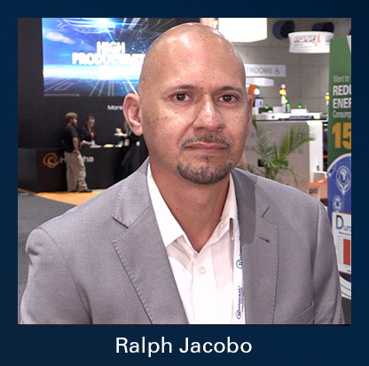
In a rapidly evolving manufacturing landscape, the shift toward substrate technology has become a focal point for some companies in the PCB industry. Ralph Jacobo, technical sales and application engineer at all4-PCB, says all4-PCB has its roots in via-filling technology, has successfully navigated various market changes, and is now keenly focused on the demands of substrate manufacturing in North America. Ralph shares insights into the company's historical journey, current initiatives, and the innovative steps being taken to address the complexities of modern substrate processes.
Marcy LaRont: Ralph, tell us a little about the company’s history and development.
Ralph Jacobo: Our journey began with a heavy focus on via filling technology. In the early days, we recognized a growing demand for via-in-pad technology, which created a niche market for us. We developed partnerships with San-Ei and Tatsuta from Japan, offering non-conductive and conductive via filling materials, respectively. These early relationships were crucial in helping establish all4-PCB as a key player in the industry.
We formed strong partnerships with MASS, GroupUp, and Pola & Massa, which became staple equipment lines for the via filling and planarization processes. As the demand for epoxy via fill PCBs grew over time, we pushed the boundaries of our knowledge and capabilities to continually provide solutions tailored to the North American market leveraging our strong partnerships with equipment manufacturers.
In recent years, we’ve expanded our focus to meet the rising demand for substrate manufacturing in North America. We’re committed to staying ahead of the curve, bringing the latest technology from leading suppliers worldwide to ensure we continue to provide top-notch solutions for the North American market.
LaRont: Substrate manufacturing will be vital for the success of advanced packaging solutions. How has all4-PCB transitioned into this space?
Jacobo: It was a pretty natural progression for us. Given our extensive experience with via filling in the PCB space, we recognized that the processes for substrate manufacturing are quite similar, especially when it comes to sequential lamination cycles and the use of build-up layers.
In response to the growing demand, we discovered that our existing partners from Japan, Taiwan, and Europe were highly experienced in the substrate manufacturing process. This allowed us to expand our offerings and tap into a new and exciting field. One key difference, though, is that substrate manufacturing requires even more attention to cleanliness, material handling, and preparation, especially due to the high-density microvias involved.
To read this entire conversation, which appeared in the March 2025 issue of PCB007 Magazine, click here.


