


 Beyond the Board: Early Engagement Means Faster Prototyping for Defense Programs
 Defense Speak Interpreted: The Autonomous Plane Battle—Skyborg Vs. Loyal Wingman
 American Made Advocacy: Congress Back from Break With Work To Do


PCBAIR Invests in AI to Enhance Defect Prediction in PCB Manufacturing
April 11, 2025 | PRNewswireEstimated reading time: 1 minute
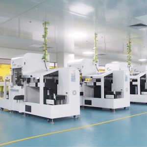
PCBAIR, a leading provider of PCB manufacturing and assembly services with fully automated production lines, announced that it is increasing funding for research and development to incorporate AI into its manufacturing processes, dramatically improving defect prediction accuracy and efficiency.
"We are focused on improving our manufacturing processes," says Dr. Jian Li, Chief Technology Officer at PCBAIR. "Our investment in AI-powered defect prediction represents a major step forward. By applying machine learning and advanced thermal imaging analysis, we can identify potential defects with unprecedented precision, long before they impact product quality."
The core of PCBAIR's research centers on developing sophisticated AI algorithms trained on vast datasets of thermal images and other process data. This allows the system to learn the subtle indicators of potential defects, such as solder joint inconsistencies, component misalignments, and other anomalies that might be missed by traditional inspection methods.
"This technology has the potential to transform how we approach quality control," adds Sarah Chen, Director of Quality Assurance at PCBAIR. "Instead of simply reacting to defects, we can proactively address them, ensuring that every circuit board we produce meets the highest standards of performance and reliability. This is particularly crucial for our customers in demanding sectors like aerospace, medical devices, automotive electronics, and industrial automation, where failure is not an option."
PCBAIR's research also incorporates the integration of AI-driven insights with its existing automated production lines, creating a closed-loop system for continuous improvement. The company anticipates that this technology will not only enhance its own manufacturing capabilities but also provide valuable data for optimizing PCB design and component selection in the future. The aim is making the whole ecosystem from design to manufacture more robust.
Share on:


Testimonial
"In a year when every marketing dollar mattered, I chose to keep I-Connect007 in our 2025 plan. Their commitment to high-quality, insightful content aligns with Koh Young’s values and helps readers navigate a changing industry. "
Brent Fischthal - Koh YoungSuggested Items
EMS Solutions Expands Workforce to Meet Rising Demand for U.S.-Based Electronics Manufacturing
10/17/2025 | EMS SolutionsEMS Solutions, a premier regional provider of Electronics Manufacturing Services (EMS), has announced several new hires across key departments as the company continues to grow its capabilities and meet increasing customer demand.
Jabil Announces Board Transitions
10/17/2025 | JabilJabil Inc. announced that Executive Chairman of the Board of Directors Mark T. Mondello and Directors Kathleen A. Walters and Jamie Siminoff will not seek re-election at Jabil’s Annual Meeting of Stockholders in January 2026.
StenTech Strengthens Precision Parts Platform with AME Acquisition
10/17/2025 | StenTechStenTech, North America’s leading provider of SMT printing solutions and precision manufacturing, has announced the acquisition of Advanced Metal Etching, Inc. (AME), a recognized specialist in chemically etched and laser cut precision parts.
MKS’ Atotech, ESI to Participate in TPCA Show & IMPACT Conference 2025
10/17/2025 | MKS’ AtotechMKS Inc., a global provider of enabling technologies that transform our world, announced that its strategic brands Atotech (process chemicals, equipment, software, and services) and ESI (laser systems) will showcase their latest range of leading manufacturing solutions for printed circuit board (PCB) and package substrate manufacturing at the upcoming 26th TPCA Show 2025 to be held at the Taipei Nangang Exhibition Center from 22-24 October 2025.
Primax, Vieureka Partner to Drive Next-Generation EDGE AI
10/17/2025 | PRNewswirePrimax Electronics Ltd., a leading global ODM with AI sensor fusion technologies, and Vieureka Inc., a Japanese edge AI innovator, announced a strategic partnership to develop a next-generation edge AI camera.