


 Global PCB Connections: Rigid-flex and Flexible PCBs—The Backbone of Modern Electronics
 Flexible Thinking: The Key to a Successful Flex Circuit Design Transfer
 Happy’s Tech Talk #29: Bend-to-Install Semi-flex FR-4


Real Time with... IPC APEX EXPO 2025: Emerging Trends in Design and Technology
April 16, 2025 | Real Time with...IPC APEX EXPOEstimated reading time: Less than a minute
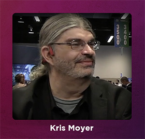
Andy Shaughnessy speaks with IPC design instructor Kris Moyer to discuss emerging design trends. They cover UHDI technology, 3D printing, and optical data transmission, emphasizing the importance of a skilled workforce. The role of AI in design is highlighted, along with the need for understanding physics and mechanics as designs become more complex. The conversation concludes with a focus on enhancing math skills for better signal integrity.
The 25th IPC APEX EXPO, March 18-20, 2025, at the Anaheim Convention Center in California, has concluded successfully. If you couldn’t make it to the show, don’t worry—the I-Connect007 team has coverage of the entire week’s events. Don’t miss our Real Time with… IPC APEX EXPO 2025 video interviews with the movers and shakers of the electronics industry.
Share on:


Testimonial
"Your magazines are a great platform for people to exchange knowledge. Thank you for the work that you do."
Simon Khesin - Schmoll MaschinenSuggested Items
RT-Labs Joins STMicroelectronics Partner Program to Accelerate Industrial Communication
10/16/2025 | RT-LabsRT-Labs, a leading provider of real-time software solutions for industrial automation, announces that it has joined the STMicroelectronics Partner Program to integrate its Ethernet-based industrial communication stacks into ST’s development environments and microcontroller platforms.
ASC Sunstone Circuits Adds New Options to OneQuote While Maintaining Real-Time Pricing on Core PCB Features
10/16/2025 | ASC Sunstone CircuitsASC Sunstone Circuits, a leading U.S. PCB manufacturer, today announced a significant expansion of its OneQuote online quoting tool, giving design engineers more control over complex PCB configurations — making it easier for the quote team to quickly clarify and verify specifications, reducing delays from manual quote reviews.
Analog Devices Launches ADI Power Studio™ and New Web-Based Tools
10/14/2025 | Analog Devices, Inc.Analog Devices, Inc., a global semiconductor leader, announced the launch of ADI Power Studio, a comprehensive family of products that offers advanced modeling, component recommendations and efficiency analysis with simulation. In addition, ADI is introducing early versions of two new web-based tools with a modernized user experience under the Power Studio umbrella:
Cadence Giving Foundation Announces Multi-Year Commitment to Expand the AI Hub at San José State University
10/13/2025 | Cadence Design Systems, Inc.The Cadence Giving Foundation today announced a multi-year commitment to expand the AI Hub at San José State University (SJSU) to equip students with the skills, hands-on training and experience needed to excel in careers in artificial intelligence (AI).
NEDME Returns October 22 — The Northwest’s Premier Design & Manufacturing Expo
10/13/2025 | NEDMEThe Northwest Electronics Design & Manufacturing Expo (NEDME) returns on Wednesday, October 22, 2025, at Wingspan Event & Conference Center, Hillsboro. The event brings together engineers, product designers, manufacturers, educators, and community partners for a full day of industry connection, learning, and networking.