-

- News
- Books
Featured Books
- smt007 Magazine
Latest Issues
Current Issue
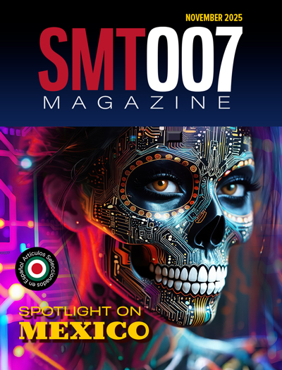
Spotlight on Mexico
Mexico isn’t just part of the electronics manufacturing conversation—it’s leading it. From growing investments to cross-border collaborations, Mexico is fast becoming the center of electronics in North America. This issue includes bilingual content, with all feature articles available in both English and Spanish.

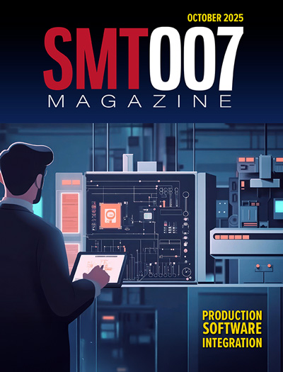
Production Software Integration
EMS companies need advanced software systems to thrive and compete. But these systems require significant effort to integrate and deploy. What is the reality, and how can we make it easier for everyone?

Spotlight on India
We invite you on a virtual tour of India’s thriving ecosystem, guided by the Global Electronics Association’s India office staff, who share their insights into the region’s growth and opportunities.
- Articles
Article Highlights
- Columns
- Links
- Media kit
||| MENU - smt007 Magazine
Lam Research Donates Leading-Edge Etch System to Accelerate Nanofabrication R&D at UC Berkeley
April 17, 2025 | PRNewswireEstimated reading time: 2 minutes
Lam Research Corp. announced the donation of its innovative multi-chamber semiconductor etching system to the Marvell Nanofabrication Laboratory at the University of California, Berkeley to advance research and development (R&D) for next-generation chip technologies. Through Lam's donation, frontline researchers can now have access to a state-of-the-art etching system for fabricating nanoscale semiconductor devices, including Specialty Technologies, that are needed to support a wide range of applications — from consumer and industrial electronics to artificial intelligence (AI) and quantum computing hardware.
The Berkeley Marvell NanoLab is a shared research center providing cross-departmental principal investigators and hundreds of academic and industrial researchers with access to micro- and nano-fabrication technologies typically only found in modern fab facilities. Lam's latest contribution builds on the company's long history of collaboration with UC Berkeley to expand research and educational activities in nanoscale science and engineering to accelerate the pace of innovation for semiconductor manufacturing.
"We believe that academia-industry collaboration is crucial to driving the nanofabrication advancements needed for new generations of Specialty Technologies," said Vahid Vahedi, chief technology and sustainability officer at Lam Research. "Lam's donation will give UC Berkeley's NanoLab researchers the ability to work directly with an industry-proven semiconductor manufacturing system in their efforts to accelerate innovation and develop new, novel processes."
The system combines Lam's Kiyo® conductor and metal etch, Flex® dielectric etch, and a state-of-the-art Syndion® GP deep reactive ion etch chambers on a Lam 2300® platform. It is capable of etching a broad range of materials needed for manufacturing next-generation semiconductor devices and advancing Specialty Technology applications such as optoelectronics and photonics, sensors and radio frequency (RF) solutions.
In addition to Lam's donation, the company's ongoing collaboration with UC Berkeley includes funding of foundational research within the College of Engineering. Lam's etch technologies will enable expanded pathfinding in new fabrication processes for integrated optical solutions such as switches, waveguides, electro optic modulators and fiber coupling technologies. Such optical elements are critical building blocks in the advancement of photonic integrated circuits and optical interconnects, solutions that are expected to serve as critical enablers for applications including optical communications, advanced AI hardware, data center infrastructure and quantum information processing.
"We thank Lam Research for its many contributions over the years to UC Berkeley's Marvell NanoLab in support of research and innovation for nanofabrication technologies," said Tsu-Jae King Liu, dean of UC Berkeley's College of Engineering. "Lam's latest donation gives our researchers and students access to wafer-processing capabilities rarely accessible outside of the most sophisticated semiconductor manufacturing facilities. I look forward to seeing Lam's advanced etching system enable new atomic-scale innovations for next-generation chips in the years ahead."
Testimonial
"Advertising in PCB007 Magazine has been a great way to showcase our bare board testers to the right audience. The I-Connect007 team makes the process smooth and professional. We’re proud to be featured in such a trusted publication."
Klaus Koziol - atgSuggested Items
Celestica Recognized Among Lam Research’s 2024 Supplier Excellence Award Winners
10/03/2024 | CelesticaCelestica Inc., a leader in design, manufacturing, hardware platform and supply chain solutions for the world’s most innovative companies, today announced that its Johor, Malaysia operation was honoured with a 2024 Supplier Excellence Award from Lam Research, a global provider of innovative wafer fabrication equipment and services to the semiconductor industry.
Bioinspired Technology
01/26/2016 | UC Santa BarbaraThe next great technological advance in smartphone screens and solar cells could come from an unexpected source — giant clams. New research from UC Santa Barbara shows some species of these large bivalves produce their white coloration via color-mixing techniques akin to those used in reflective displays.
In-Circuit Pin Testing: An Excellent Potential Source of Value Creation
06/17/2015 | Mitch Holtzer, AlphaIn-circuit pin testing (ICT) is a common method of inspecting electronic assemblies to measure the effectiveness of the assembly process and to predict electrical functionality. In this article, Mitch Holtzer talks about ICT and how its accuracy can bring significant competitive advantage to assemblers. He also provides an example of doing ICT in an assembly.


