


 Trouble in Your Tank: Implementing Direct Metallization in Advanced Substrate Packaging
 It’s Only Common Sense: Storytelling That Sells—Stop Pitching, Start Painting Pictures
 The Right Approach: Get Ready for ISO 9001 Version 6


Autodesk Donates $4.3 Million to Cornell University to Prepare students for an AI-powered future
April 24, 2025 | AutodeskEstimated reading time: 3 minutes
Autodesk announced a $4.3 million gift to Cornell University’s College of Engineering and College of Architecture, Art, and Planning (AAP) to help prepare students for the future of work in an increasingly AI-driven world. The investment will fund a new Autodesk Cornell Engineering Design and Make Space in Upson Hall.
This interdisciplinary facility will serve as a hub for experiential learning, where students can prototype, collaborate, and build using the same advanced tools and platforms as industry professionals—including free access to Autodesk Fusion, an all-in-one platform for CAD, CAM, and generative design.
“The world urgently needs skilled talent to design and make the brighter future we know is possible—but right now, there’s a critical skills gap,” said Dara Treseder, Chief Marketing Officer at Autodesk. “Autodesk is committed to closing this gap by putting cutting-edge technology directly into the hands of tomorrow’s innovators. Our collaboration with Cornell University accelerates this effort, equipping the next generation of engineers, architects, and designers with the tools, technology, and real-world experience they need to build successful careers and shape our collective future.”
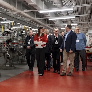
Cornell’s J. Meejin Yoon, Gale and Ira Drukier Dean of Architecture, Art, and Planning; Lynden A. Archer, Joseph Silbert Dean of Engineering; and Krystyn Van Vliet, Vice President for Innovation and External Engagement Strategy, join Autodesk’s Jeff Kinder, Executive Vice President of Product Development and Manufacturing Solutions, and Ruth Ann Keene, Executive Vice President of Corporate Affairs and Chief Legal Officer, for the official signing of the memorandum of understanding facilitated by robotic arms in AAP’s Autodesk Design and Make Space. Anson Wigner / AAP
Closing the skills gap
The announcement coincides with the release of Autodesk’s 2025 State of Design & Make report, which found that AI is now the number one skill employers are hiring for across Design and Make industries. Meanwhile, 61% of industry professionals say new employees with the right technical skills are difficult to find, up 16 points from last year.
Autodesk’s long-standing collaboration with Cornell directly addresses this challenge and focuses on helping students across architecture, engineering, and more develop the right skillsets for jobs of the future.
As part of this gift, Cornell Engineering and AAP will each receive $2 million to enhance fabrication labs, research spaces, and prototyping tools, plus $150,000 in discretionary funds to accelerate innovation and instruction.
“The Autodesk Design and Make Space in Cornell Engineering is an investment in the future of experiential learning in our college that impacts students college-wide,” said Lynden Archer, Joseph Silbert Dean of Engineering. “I am grateful for and encouraged by Autodesk’s support of our efforts to educate problem solvers with combined hands-on and computational design expertise, which is critical in modern engineering and design practice.”
Equipping students to build a sustainable future
At the College of Architecture, Art, and Planning, Autodesk’s donation names the AAP Autodesk Design and Make Space, which encompasses the current fabrication shops in Rand Hall. It will also enhance other maker spaces in the college, support research into emerging technologies, and align with growing student demand for green jobs and sustainable design education.
And the need has never been clearer:
- 3 in 4 professionals at tech-advanced companies say sustainability efforts help attract and retain top talent.*
- Nearly half of college students say they want to pursue a career in sustainability — but need the skills and training to get there.**
“At AAP, teaching, research, and learning thrive in environments that scaffold creativity, innovation, and iteration and encourage fluidity between digital and analog techniques,” said J. Meejin Yoon, Gale and Ira Drukier Dean of AAP. “This generous contribution to our college enables us to see that our spaces for creation and fabrication remain at the forefront and enable opportunities for collaboration across fields. Helping to further AAP’s mission, Autodesk’s gift ensures our faculty are well-supported, and our students are prepared to drive transformation across our disciplines with the resources, tools, and technologies needed to both inspire and actualize imagination.”
Why it matters now
As industries evolve at the speed of technology, the workforce is struggling to keep up. According to Autodesk’s 2025 State of Design & Make report:
- 46% of employers say AI skills are a top hiring priority.
- 58% say a lack of skilled talent is a barrier to their company’s growth—up 15 points from last year.
Autodesk’s investment is designed to help close that gap—giving students the technology, training, and experience to thrive in a world shaped by AI, sustainability, and innovation.
Share on:


Testimonial
"Advertising in PCB007 Magazine has been a great way to showcase our bare board testers to the right audience. The I-Connect007 team makes the process smooth and professional. We’re proud to be featured in such a trusted publication."
Klaus Koziol - atgSuggested Items
ASM Technologies Limited signs MoU with the Guidance, Government of Tamilnadu to Expand Design-Led Manufacturing capabilities for ESDM
09/15/2025 | ASM TechnologiesASM Technologies Limited, a pioneer in Design- Led Manufacturing in the semiconductor and automotive industries, announced signing of Memorandum of Understanding (MoU) with the Guidance, Government of Tamilnadu whereby it will invest Rs. 250 crores in the state to expand its ESDM related Design-Led Manufacturing and precision engineering capacity. ASM Technologies will acquire 5 acres of land from the Government of Tamilnadu to set up a state-of-the-art design facility in Tamil Nadu's growing technology manufacturing ecosystem, providing a strong strategic advantage and long-term benefits for ASM.
Variosystems Strengthens North American Presence with Southlake Relaunch 2025
09/15/2025 | VariosystemsVariosystems celebrated the relaunch of its U.S. facility in Southlake, Texas. After months of redesign and reorganization, the opening marked more than just the return to a modernized production site—it was a moment to reconnect with our teams, partners, and the local community.
Deca, Silicon Storage Technology Announce Strategic Collaboration to Enable NVM Chiplet Solutions
09/11/2025 | Microchip Technology Inc.As traditional monolithic chip designs grow in complexity and increase in cost, the interest and adoption of chiplet technology in the semiconductor industry also increases.
I-Connect007 Launches New Podcast Series on Ultra High Density Interconnect (UHDI)
09/10/2025 | I-Connect007I-Connect007 is excited to announce the debut of its latest podcast series, which shines a spotlight on one of the most important emerging innovations in electronics manufacturing: Ultra-High-Density Interconnect (UHDI). The series kicks off with Episode One, “Ultra HDI: What does it mean to people? Why would they want it?” Host Nolan Johnson is joined by guest expert John Johnson, Director of Quality and Advanced Technology at American Standard Circuits (ASC).
Global Citizenship: Together for a Perfect PCB Solution
09/10/2025 | Tom Yang -- Column: Global CitizenshipIf there’s one thing we’ve learned in the past few decades of electronics evolution, it’s that no region has a monopoly on excellence. Whether it’s materials science breakthroughs in Europe, manufacturing efficiencies in China, or design innovations in Silicon Valley, the PCB industry thrives on collaboration.