


 The Right Approach: The Pros and Cons of PCB Vertical Integration
 American Made Advocacy: PCBAA’s Fifth Annual Meeting—Growing Membership and Valuable Relationships
 It's Only Common Sense: Why the Best Years of Electronics Are Still Ahead of Us


Driving Innovation: Registration in PCB Production Throughout the Process
PCB manufacturing is a fascinating industry where multiple disciplines—chemical, mechanical, and optical processes—intersect. Each field plays a crucial role, and missing even one step can significantly impact production and yield.
In the realm of mechanical and optical processes, one of the most critical aspects influencing the final result—especially in complex PCB designs—is registration.
I often compare the PCB registration process to assembling a cheeseburger. You wouldn’t want your tomato sliding off one side, the patty leaning in the opposite direction, and the cheese hanging unevenly. A well-made burger should be neatly stacked and precisely aligned so that every bite delivers the perfect balance of flavors. The same applies to PCB registration—inner layers should be aligned as well as possible. While achieving perfect alignment is impossible, the key is controlling tolerances to ensure consistency and precision.
This article will explore the fundamental questions:
- What are the critical registration points in PCB production?
- How can we improve alignment throughout the process?
Inner Layer Exposure
Before the introduction of direct imaging (DI) machines, contact exposure was the standard method. This process relied heavily on the alignment of phototools, making the overall accuracy dependent on the phototool's condition.
With direct imaging technology, dependency on phototools has been eliminated, but achieving proper alignment now relies fully on machines.
Since inner layers typically lack holes or fiducials—just copper—alignment must be established only by the machine itself. Modern direct imaging equipment uses small UV markers integrated into the table, exposing fiducials from the bottom side while the main exposure system processes the top side (Figure 1). These fiducials later serve as reference points after flipping the panel.
Alignment of the Inner Layers
There are multiple methods for aligning inner layers before lamination. The three primary approaches are:
- Pin-lam: Pins in the press tools hold layers in position during lamination.
- Mass-lam (without pins in press-tools during the lamination): Layup before lamination could be done using:
- A fully automated lay-up machine
- A two-step lay-up process:
- a. First machine drills registration holes.
- b. The operator stacks the layers and prepreg on pins of second machine, then performs lay-up (via welding, riveting, etc.), and user removes the stack from the pins.
Each method is viable, but the choice depends on several factors:
- Required productivity levels
- Pre- and post-processing needs
- Accuracy requirements
- Panel sizes
- Compatibility with different materials
- Capability to measure inner layers before lay-up
- Maintenance requirements
This topic alone needs a deeper discussion, and we will explore it further in future articles.
X-ray
After lamination, if pin-lam holes are not available or not used, X-ray registration is typically used to create base holes for alignment during drilling.
While some CCD-based methods exist, they require cutting through the top copper layer until the CCD can recognize internal fiducials—more common in prototyping or small production batches.
Why is X-ray Critical?
X-ray is the major control point in PCB production where we can analyze how layers behave after lamination. Misalignment can occur due to:
- PCB design factors (symmetrical or not, copper density, stack)
- Material properties (type of the material, new or stored)
- Lamination process settings
- Equipment used for inner-layer alignment and for lamination
- Pre-treatment steps (oxidation, thermal stabilization, etc.)
Fiducial Types in X-ray Registration
Two primary fiducial methods exist:
- Pad-stack fiducials: Fiducials on all layers are stacked on each other. This is faster but doesn’t provide individual layer data (Figure 2).
- Layer-to-layer fiducials: Each layer is evaluated independently, offering better accuracy and process control, especially for complex boards (Figure 3).
Optimizing X-ray Detection
If you’ve ever had an X-ray at a hospital, you know that while the image is essential for diagnosis, interpreting it requires a trained specialist. Most of the time, it’s difficult for an untrained eye to recognize details in the scan. However, in PCB manufacturing, an X-ray machine must be capable of quickly and accurately detecting fiducials without human intervention.
For the software to recognize fiducials efficiently, achieving high contrast and clear image quality is critical. Poor contrast can lead to misalignment issues, affecting the entire registration process. Several machine-specific factors play a role in optimizing fiducial detection, including:
- Machine construction to ensure stable and repeatable measurements
- X-ray source settings to enhance clarity and contrast
- Image processing algorithms for precise fiducial recognition
Figure 4a shows an example of fiducial detection on a 74-layer PCB with a 10 mm thickness, using layer-to-layer fiducials; an example of HDI board with pad-stack fiducial is shown in Figure 4b.
Another key function in X-ray registration is the ability to align to specific internal layers when needed. Ensuring the X-ray system supports this feature is critical for certain applications.
How is X-ray Data Used?
Once X-ray measurement data is available, it serves two equally important purposes in the PCB production process:
- Compensating inner-layer exposure for the next batch: By analyzing registration deviations, manufacturers can adjust exposure parameters in subsequent similar production batches to improve alignment and reduce errors over time.
- Correcting the drilling program for the current batch: X-ray data is used to align the drilling process to the actual position of the inner layers, ensuring greater accuracy in via and hole placement.
While exposure correction helps refine the overall process for future batches, drilling compensation is essential for achieving high precision within the same production batch.
To perform corrections at the drilling stage, X-ray data (needed corrections for the drilling part program to better correspond to the position of the inner layers) must be somehow transferred accurately to the drilling machine. While data can be passed manually or through specialized software, these methods have limitations—they allow data to transfer to the drilling machine but do not enable per-station compensation.
Ensuring precise alignment at each station requires a more advanced process. In such a process, aside from drilling on X-ray two positioning base holes for the prism and slot, additional holes/fiducials for the individual alignment must also be drilled directly on the X-ray machine. This allows the CCD cameras on the drilling machines to recognize those reference holes at the panel alignment level or, if needed, within individual PCB zones. In such a process, the “data about the inner layers” (i.e., needed corrections for the drilling program) can be transferred to each individual station of the drilling machine indirectly via reference fiducials/holes that are drilled on the X-ray machine in positions which correspond to the inner layer misalignment picture.
For multi-zone alignment, where a single panel contains multiple high-accuracy PCBs, the X-ray system must support full-table measurement and drilling, ensuring optimal registration across the entire panel. If multi-zone alignment is used, fiducials should be drilled not only at the panel corners but also in corners of each zone, allowing zone-specific compensation.
Mechanical Drilling Alignment
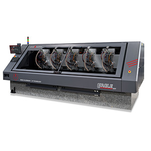
Achieving precise registration on drilling machines requires CCD cameras for fiducial recognition (Figure 5). To achieve this on multi-station machines:
- Each station must have independent CCD
- A fully independent axis system is required
Laser Alignment
Laser machines follow a similar registration approach when alignment holes are available. However, in cases where no alignment holes exist, a specialized process is required:
- The laser skives the top copper layer, also removing a small portion of the dielectric.
- The CCD camera of the laser machine then recognizes inner-layer fiducials for alignment and proceeds with the main part program drilling.
Process engineers must carefully adjust skiving parameters to ensure the laser does not penetrate deeper than the required reference layer (Figure 6).
Outer Layer Exposure Alignment
Outer layers are typically aligned using X-ray-drilled holes or holes created during main drilling.
However, when PCBs contain both mechanical and laser-drilled holes, an additional approach can be used:
Combo targets are a mechanically-drilled fiducial combined with multiple laser-drilled fiducials to create a hybrid alignment point. The direct imaging machine then aligns optimally to both reference types for maximum accuracy (Figure 7).
Solder Mask Exposure Alignment
Solder mask alignment sometimes presents additional challenges due to:
- Low-transparency solder masks (black, white, etc.)
- Partial fiducial coverage by the solder mask
Proper CCD lighting settings are crucial in overcoming these issues. With the right machine configuration and illumination adjustments, these challenges can be effectively managed (Figure 8).
Summary
In this article, we have explored registration in PCB manufacturing, a critical factor influencing yield and precision. Registration is interconnected with mechanical and optical processes, impacting nearly every step of PCB fabrication.
As PCB designs continue to evolve, achieving precise registration will remain a key challenge—one that requires both advanced technology and a deep understanding of process control.
This column originally appeared in the April 2025 issue of PCB007 Magazine.


