-
- News
- Books
Featured Books
- smt007 Magazine
Latest Issues
Current IssueSupply Chain Strategies
A successful brand is built on strong customer relationships—anchored by a well-orchestrated supply chain at its core. This month, we look at how managing your supply chain directly influences customer perception.
What's Your Sweet Spot?
Are you in a niche that’s growing or shrinking? Is it time to reassess and refocus? We spotlight companies thriving by redefining or reinforcing their niche. What are their insights?
Moving Forward With Confidence
In this issue, we focus on sales and quoting, workforce training, new IPC leadership in the U.S. and Canada, the effects of tariffs, CFX standards, and much more—all designed to provide perspective as you move through the cloud bank of today's shifting economic market.
- Articles
- Columns
- Links
- Media kit
||| MENU - smt007 Magazine
ZETWERK Enhances Manufacturing Capabilities with TRI
June 4, 2025 | TRIEstimated reading time: Less than a minute

Test Research, Inc. (TRI), the leading test and inspection systems provider for the electronics manufacturing industry, is pleased to announce that ZETWERK Electronics has integrated TRI's Automated Optical Inspection (AOI) and Solder Paste Inspection (SPI) solutions into its state-of-the-art manufacturing facility in Tamil Nadu. These advanced inspection solutions were delivered through TRI's trusted distributor in India, Test & Research India.
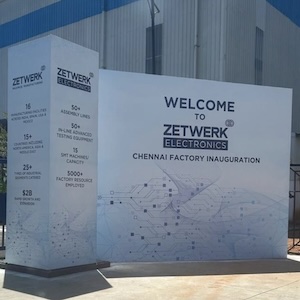
The grand inauguration of ZETWERK Electronics' cutting-edge manufacturing facility in Thiruvallur marks a significant advancement in India's electronics manufacturing sector, reinforcing the country's growing influence in the global supply chain.
By integrating TRI's AOI and SPI solutions, ZETWERK ensures the highest standards of precision, efficiency, and quality in its production processes. These advanced systems enhance manufacturing accuracy, reduce defects, and optimize production workflows.
Testimonial
"In a year when every marketing dollar mattered, I chose to keep I-Connect007 in our 2025 plan. Their commitment to high-quality, insightful content aligns with Koh Young’s values and helps readers navigate a changing industry. "
Brent Fischthal - Koh YoungSuggested Items
Target Condition: Floor Planning Without a Floor
08/27/2025 | Kelly Dack -- Column: Target ConditionBy a show of hands, how many PCB designers have been asked to start a layout without a board outline, keep-out zones, or even height constraints? How many have had to work within a specific enclosure before the schematic was finalized? If this sounds familiar, you're not alone. Starting a PCB layout without critical constraints is like hiring an interior designer to buy furniture and carpet for a house you haven’t even purchased yet, or, even worse, trying to fit four bedrooms' worth of furniture in a one-room cabin.
TRI: Discover SEMI Inspection and Metrology at SEMICON India 2025
08/20/2025 | TRITest & Research India PVT, LTD. (T&R India), TRI's distributor, will join SEMICON India 2025 at Yashobhoomi (IICC), New Delhi, India from September 2 – 4, 2025.
TRI's One-Stop Solutions at SMTA Michigan and Long Island 2025
08/18/2025 | TRITest Research, Inc. (TRI), the leading provider of test and inspection systems for the electronics manufacturing industry, will join SMTA Michigan and SMTA Long Island 2025.
Polymatech Electronics Limited Announces Completion of PCB Manufacturing Facility in Europe
08/15/2025 | PR NewswirePolymatech Electronics Limited is thrilled to announce the successful commissioning of its state-of-the-art Printed Circuit Board (PCB) manufacturing facility in Estonia, Europe. This milestone represents a significant advancement in the company's strategic expansion across the European market.
20 Years of Center Nanoelectronic Technologies (CNT) – Backbone of German Semiconductor Research Celebrates Anniversary
08/14/2025 | Fraunhofer IPMSThe Center Nanoelectronic Technologies (CNT) of the Fraunhofer Institute for Photonic Microsystems (IPMS) is celebrating its 20th anniversary this year. Since its founding in 2005, it has developed into a pillar of applied semiconductor research in Germany and Europe. With its unique research cleanroom and equipment adhering to the 300-mm wafer industry standard, CNT is unparalleled in Germany and serves as a central innovation driver for the microelectronics industry.