


 It’s Only Common Sense: Your Biggest Competitor Is Complacency
 The Chemical Connection: Onshoring PCB Production—Daunting but Certainly Possible
 Marcy’s Musings: The Legislative Outlook—Helping or Hurting?


Semiconductors Get Magnetic Boost with New Method from UCLA Researchers
July 31, 2025 | UCLA NewsroomEstimated reading time: 3 minutes
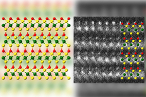
A new method for combining magnetic elements with semiconductors — which are vital materials for computers and other electronic devices — was unveiled by a research team led by the California NanoSystems Institute at UCLA.
The investigators demonstrated the ability to produce semiconductor materials containing up to 50% magnetic atoms, whereas current methods are often limited to a concentration of magnetic atoms no greater than 5%. Using their process, the team created a library of more than 20 new materials that combined magnetic elements such as cobalt, manganese and iron with a variety of semiconductors.
The study also showed that the new strategy could be used to incorporate magnetic elements into superconductors, a class of materials that allow electrons to travel through them with zero resistance under certain conditions. Other experiments added magnetic atoms to topological insulators, which are substances that behave as insulators in their interior but allow electrons to flow freely on their surface.
In tests that included the use of atomic imaging and magnetization measurements, the researchers found evidence that the new materials made with superconductors and topological insulators maintained their exotic traits while developing new magnetic behavior.
BACKGROUND
The quest to integrate magnetism into semiconductors is decades old but has yielded only modest success so far. Current techniques involve substituting a small portion of atoms in semiconductors with magnetic atoms. However, above a critical concentration threshold of about 5%, the magnetic atoms tend to clump in a way that undermines the capacity to control the materials’ magnetic and electronic properties.
Semiconductors with controllable magnetic properties could be the basis for spintronics (technologies that operate based on a property of electrons called spin), similarly to how traditional electronics operate based on electrons’ charge. Spin offers a new way to store and process information by using the direction an electron spins — either “up” or “down” — like tiny bar magnets flipping north or south.
Spintronics are already used in technologies such as the read heads that pull data off the hard drives in computers and other devices. Unlike conventional electronics, spintronic components don’t produce excess heat, a major barrier to cramming more power into smaller chips. By overcoming this limitation, spintronics could lead to future devices that are more powerful, compact and energy-efficient, or even ones with entirely new capabilities.
Magnetic materials produced with the new method might also serve as foundational materials for future quantum computers. Such devices are expected to complete calculations that are currently impossible, to simulate complex natural phenomena at a level that traditional computers fail to achieve, and to allow for unbreakable cybersecurity.
METHOD
The researchers’ technique involves alternately stacking together atomically thin sheets of the semiconductors and self-organized layers of magnetic atoms. This layered architecture allows each component to retain its ordered arrangements and intrinsic properties while giving rise to new collective behaviors.
IMPACT
The team’s process could provide a versatile material platform for future spintronic devices that can do more than contemporary electronics, with superior energy efficiency. For example, today’s popular artificial intelligence systems consume enormous amounts of electricity and water; future computers deploying spintronics may host AI applications that are more powerful while avoiding the worrying carbon footprint and drain on vital resources.
Exotic materials that combine semiconductor or superconductor properties with magnetism could also help raise the temperature at which quantum computers operate to more practical levels — unlike current systems that require extremely cold conditions.
Deployed in basic research, new materials combining semiconductors and magnetism could help improve the understanding of fundamental forces and interactions underlying not only advanced technology but also nature itself.
Share on:


Testimonial
"Your magazines are a great platform for people to exchange knowledge. Thank you for the work that you do."
Simon Khesin - Schmoll MaschinenSuggested Items
Elementary Mr. Watson: Chasing Checkmarks, Not Signal Integrity
10/01/2025 | John Watson -- Column: Elementary, Mr. WatsonFor the September 2025 issue of Design007 Magazine on signal integrity, I explored how the PCB is similar to a military obstacle course: walls that sap energy like impedance mismatches, barbed wire that cuts like crosstalk, and mud pits that drag a signal down like attenuation. The takeaway was clear that a PCB is not a flat drawing; it's an electromagnetic ecosystem filled with hazards that test every signal that dares to cross it. The real danger lies not in the obstacles themselves, but in the fact that many designers never see them.
Honeywell Awarded U.S. Government Contracts to Develop Quantum Sensor-Based Navigation Systems
07/21/2025 | HoneywellHoneywell has been selected by the U.S. Department of Defense’s (DOD) Defense Innovation Unit (DIU) to participate in the Transition of Quantum Sensing (TQS) program.
Leidos Using Quantum Technology to Thwart GPS Jamming
06/05/2025 | PRNewswireSusceptibility to jamming is a significant military vulnerability of the Global Positioning System (GPS) signal. Through a Defense Innovation Unit contract, Leidos is developing an alternative navigation technology that measures variations in the Earth's magnetic field and harnesses the quantum properties of nitrogen in diamonds.
Beyond Design: Radiation and Interference Coupling
05/21/2025 | Barry Olney -- Column: Beyond DesignRadiation and interference coupling pose significant challenges to the performance and reliability of high-speed digital designs. Whether it's the unintended emission of electromagnetic waves or the interaction of signals between adjacent circuits, these phenomena can lead to unwanted noise, signal distortion, and even system malfunctions. Understanding the mechanisms behind radiation and interference coupling is crucial for electronics designers seeking to design robust and efficient systems.
Mycronic’s Global Technologies Makes Acquisition in France
03/13/2025 | MycronicMycronic’s Global Technologies division has acquired Hprobe, a company headquartered in Grenoble, France, which has developed a unique technology for high-speed magnetic testing of Magnetoresistive Random Access Memories (MRAMs) and magnetic sensors.