


 Trouble in Your Tank: At 40 GHz, Everything Matters, Part 2
 It’s Only Common Sense: Stop Watching the Headlines and Start Watching the Opportunity
 The Right Approach: The Pros and Cons of PCB Vertical Integration


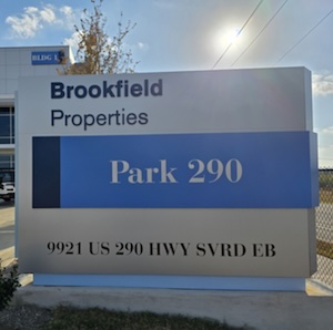
Specialized Packaging Group (SPG), a leading provider of sustainable protective packaging solutions, announced the opening of a new Austin-area manufacturing facility. The new 75,000-square-foot site expands the company’s custom-engineered packaging capabilities and strengthens service for customers across the southern and mid-south regions of the U.S.
Located in northeast Austin, the facility strengthens the company’s ability to deliver innovative packaging solutions across a wide range of industries, with initial production focused on engineered corrugated and foam packaging for automotive and technology customers, including the server rack and semiconductor markets.
“The Austin facility represents a strategic milestone for SPG,” said Joe Gumbis, Chief Commercial Officer, SPG. “This site allows us to better support some of our largest customers, respond faster to regional demand and it reinforces our commitment to being in proximity to our customers.”
The facility is equipped with advanced manufacturing technology, including a state-of-the-art rotary die cutter and dual-color printing system, as well as SPG’s first cold-glue automated system for corrugated applications. These capabilities enable the production of highly customized packaging solutions tailored to customers’ specific performance and protection requirements.
As part of its commitment to regional engagement and responsible operations, the Austin facility is creating new jobs in the community and is prioritizing partnerships with local vendors and service providers.
“Establishing this site has been a true team effort,” Gumbis said. “From sourcing local partners to building our workforce, we’re proud to be contributing to the Austin community while delivering the level of quality and service our customers expect.”


