





















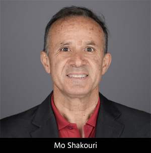
Advanced packaging and 3D heterogeneous integration are rapidly redefining the next phase of the semiconductor industry, delivering unprecedented performance gains while posing significant thermal management challenges. In this interview, Dr. Mohammad (Mo) Shakouri, founder and CEO of Microsanj, discusses how thermoreflectance-based metrology is enabling engineers to visualize and measure heat behavior at the nanoscale within complex packages, interposers, and TSV structures. He draws on decades of experience in semiconductors and photonics to explain why thermal characterization, materials innovation, and inline metrology are critical to the future reliability and performance of AI-driven electronics.
Marcy LaRont: Dr. Shakouri, it is lovely to meet you. Please tell me a little bit about yourself and Microsanj.
Mo Shakouri: I earned my PhD in physics and electronics from Stanford and have been involved in various industries: RF/microwave, semiconductor, high-speed electronics, and photonics. I've worked at Bell Labs and Hewlett-Packard, to name a couple, and I live in Silicon Valley, where so many pioneering electronics companies began.
My brother and I started Microsanj about 18 years ago as a completely different type of company. He was a professor at the University of California, Santa Cruz, where his department was developing microrefrigerators. They advanced a technique to measure them, and then we further developed it, which formed the basis of our company. We used the reflection of light to measure temperature (thermoreflectance). Typically, measuring thermal characterization has been more art than science, going into a dark room and counting emissions. So, it is unique in the industry.
We're focused on R&D, but we were a startup 15 years ahead of its time. Given what has happened in the semiconductor industry over the past five years, and the trend in which temperature and heat are critical factors, we are now considered experts. Many companies and universities are now interested in our tools and technology.
LaRont: What was the premise of your presentation at APEX EXPO titled “Meeting Emerging Thermal Challenges of 3D Heterogeneously Integrated Circuit Packaging Techniques?”
Shakouri: For 40 years, the semiconductor industry has pursued the idea, "Let me make a bigger wafer and a smaller chip." That's how the scaling happened; it was Moore's Law. Five to seven years ago, we began to see limitations arising from yields and costs.
Overcoming these limitations has led us to 3DHI packaging.
Developing these components involves many different materials that must interface and be packaged together. For example, when integrating memory, digital, and photonics, how do I stack them? Layered packaging is a newer trend in the semiconductor industry. An analogy would be like moving from building single-family homes in the 1970s and 1980s to today's high-rise luxury apartments. We’ve run out of room for more single-family homes, so we're creating more housing by building high-rise apartments.
LaRont: That is a great analogy.
Shakouri: Memory and power distribution have different biases with very sensitive elements. Heat is becoming a critical element. You used to have a big, powerful heat sink in your PCBA where the chip would be placed, but today, that is nearly impossible. How do you deal with that? How do you get rid of heat?
The answer is 3D heterogeneous integration (HI). A critical element in the temperature problem is knowing where the actual thermal problem lies within the integrated package.
LaRont: Heat has become a much greater issue due to modern power and speed demands, but isn’t that because a single 3D package requires different materials, which don't behave the same or aren't necessarily compatible from a heat perspective?
Shakouri: Correct. As memory and high power modules (HPM) have developed, they are very sensitive to temperature. Silicon has been a great material for this. But when we get to high compute, high power, and high input, we need to deal with power distribution. This is important because when you get more current from the power supply right next to the memory bits, it causes errors.
We can’t just do everything through copper. Today, people are talking about silicon photonics, leveraging gallium nitride, gallium arsenide, standard silicon, and maybe glass. Suddenly, you have mismatched materials coming together, each with different properties and thermal resistance. I call that the typical melting pot. It’s a bit like the different cultures coming together in Silicon Valley. How do you get them to communicate and work together?
That's where people are trying to optimize the design, where we are seeing new developments in materials, interposers, and package solutions, and in the development of through-silicon vias (TSVs), the vias serve as layer to layer interconnections in multi-layer package structures.
The Global Electronics Association is committed to conducting these sessions at APEX EXPO because they see trends in the packaging industry. It’s not your grandpa's semiconductor anymore. We used to joke that semiconductors were the king, and the packaging guys were the peasants who had to deal with it. Now, packaging is coming to the forefront because it must solve a fundamental problem from the beginning. That's a significant change for the industry.
LaRont: We're seeing that on the traditional PCB side as well. The divide is becoming very narrow as PCBs become increasingly dense. Add the interposer and the rest of the package, and they all have to go together in a new way.
Shakouri: Yes, and then there is the challenge of scale. Look at the AI push where you're potentially putting the amount of power to run a city inside one of these chips. The density required is unbelievable. It's pushing the whole semiconductor industry to the next level. In trying to answer the fundamental question of reliability, thermal is one of the biggest challenges. So, thermal metrology is becoming an important issue. Luckily for us, about 20 years ago, we commercialized this work and built it for ourselves because we're using it for optical imaging.
Page 1 of 2


