


 Dan’s Biz Bookshelf: ‘Dream First, Details Later
 Happy’s Tech Talk #40: Factors in PTH Reliability—Hole Voids
 Facing the Future: Time for Real Talk, Early and Often, Between Design and Fabrication


New Sensing Technology Could Improve Ability to Detect
June 10, 2015 | University at BuffaloEstimated reading time: 3 minutes
From airport security detecting explosives to art historians authenticating paintings, society’s thirst for powerful sensors is growing.
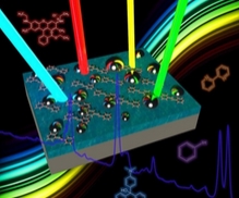
Given that, few sensing techniques can match the buzz created by surface-enhanced Raman spectroscopy (SERS).
Discovered in the 1970s, SERS is a sensing technique prized for its ability to identify chemical and biological molecules in a wide range of fields. It has been commercialized, but not widely, because the materials required to perform the sensing are consumed upon use, relatively expensive and complicated to fabricate.
That may soon change.
An international research team led by University at Buffalo engineers has developed nanotechnology that promises to make SERS simpler and more affordable.
Described in a research paper published in the journal Advanced Materials Interfaces, the photonics advancement aims to improve our ability to detect trace amounts of molecules in diseases, chemical warfare agents, fraudulent paintings, environmental contaminants and more.
“The technology we’re developing – a universal substrate for SERS – is a unique and, potentially, revolutionary feature. It allows us to rapidly identify and measure chemical and biological molecules using a broadband nanostructure that traps wide range of light,” said Qiaoqiang Gan, UB assistant professor of electrical engineering and the study’s lead author.
Additional authors of the study are: UB PhD candidates in electrical engineering Nan Zhang, Kai Liu, Haomin Song, Xie Zeng, Dengxin Ji and Alec Cheney; and Suhua Jiang, associate professor of materials science, and Zhejun Liu, PhD candidate, both at Fudan University in China.
When a powerful laser interacts chemical and biological molecules, the process can excite vibrational modes of these molecules and produce inelastic scattering, also called Raman scattering, of light. As the beam hits these molecules, it can produce photons that have a different frequency from the laser light. While rich in details, the signal from scattering is weak and difficult to read without a very powerful laser.
SERS addresses the problem by utilizing a nanopatterned substrate that significantly enhances the light field at the surface and, therefore, the Raman scattering intensity. Unfortunately, traditional substrates are typically designed for only a very narrow range of wavelengths. This is problematic because different substrates are needed if scientists want to use a different laser to test the same molecules. In turn, this requires more chemical molecules and substrates, increasing costs and time to perform the test.
The universal substrate solves the problem because it can trap a wide range of wavelengths and squeeze them into very small gaps to create a strongly enhanced light field.
The technology consists of a thin film of silver or aluminum that acts as a mirror, and a dielectric layer of silica or alumina. The dielectric separates the mirror with tiny metal nanoparticles randomly spaced at the top of the substrate.
“It acts similar to a skeleton key. Instead of needing all these different substrates to measure Raman signals excited by different wavelengths, you’ll eventually need just one. Just like a skeleton key that opens many doors,” Zhang said.
“The applications of such a device are far-reaching,” said Kai Liu. “The ability to detect even smaller amounts of chemical and biological molecules could be helpful with biosensors that are used to detect cancer, Malaria, HIV and other illnesses.”
It could be useful identifying chemicals used in certain types of paint. This could be helpful detecting forged pieces of art as well as restoring aging pieces of art. Also, the technology could improve scientists’ ability to detect trace amounts of toxins in the air, water or other spaces that are causes for health concerns. And it could aid in the detection of chemical weapons.
The National Science Foundation supported the research in a grant to develop a real-time in-vivo biosensing system. Gan shares the grant with Josep M. Jornet and Zhi Sun, both assistant professors of electrical engineering at UB.
Gan is a member of UB’s electrical engineering optics and photonics research group, which includes professors Edward Furlani, Natalia Litchinitser and Pao-Lo Liu; and assistant professor Liang Feng.
The group carries out research in nanophotonics, biophotonics, hybrid inorganic/organic materials and devices, nonlinear and fiber optics, metamaterials, nanoplasmonics, optofluidics, microelectromechanical systems (MEMS), biomedical microelectromechanical systems (BioMEMs), biosensing and quantum information processing.
Share on:


Suggested Items
Symposium Review: Qnity, DuPont, and Insulectro Forge Ahead with Advanced Materials
07/02/2025 | Barb Hockaday, I-Connect007In a dynamic and informative Innovation Symposium hosted live and on Zoom on June 25, 2025, representatives from Qnity (formerly DuPont Electronics), DuPont, and Insulectro discussed the evolving landscape of flexible circuit materials. From strategic corporate changes to cutting-edge polymer films, the session offered deep insight into design challenges, reliability, and next-gen solutions shaping the electronics industry.
Indium Corporation Expert to Present on Automotive and Industrial Solder Bonding Solutions at Global Electronics Association Workshop
06/26/2025 | IndiumIndium Corporation Principal Engineer, Advanced Materials, Andy Mackie, Ph.D., MSc, will deliver a technical presentation on innovative solder bonding solutions for automotive and industrial applications at the Global Electronics A
Gorilla Circuits Elevates PCB Precision with Schmoll’s Optiflex II Alignment System
06/23/2025 | Schmoll MaschinenGorilla Circuits, a leading PCB manufacturer based in Silicon Valley, has enhanced its production capabilities with the addition of Schmoll Maschinen’s Optiflex II Post-Etch Punch system—bringing a new level of precision to multilayer board fabrication.
Day 1: Cutting Edge Insights at the EIPC Summer Conference
06/17/2025 | Pete Starkey, I-Connect007The European Institute for the PCB Community (EIPC) Summer Conference took place this year in Edinburgh, Scotland, June 3-4. This is the second of three articles on the conference. The other two cover the keynote speeches and Day 2 of the technical conference. Below is a recap of the first day’s sessions.
American Made Advocacy: Supporting the Entire PCB Ecosystem—Materials to OEMs
06/17/2025 | Shane Whiteside -- Column: American Made AdvocacyWith the addition of RTX to PCBAA’s membership roster, we now represent the interests of companies in the entire PCB ecosystem. From material providers to OEMs, the insights of our collective members help us educate, advocate, and support legislation and policy favorable to America’s microelectronics manufacturers. The industry veterans who lead these companies provide valuable perspective, and their accumulated wisdom makes us an even stronger association.