


 Standard of Excellence: Building Excellence From the Inside Out
 Powering the Future: Why True Ceramic Circuits Are Not Just ‘Better PCBs’
 Global Sourcing Spotlight: The Global Quality Gap—Why Consistency Wins the Contract


Plastic packaged ICs, including BGAs, whether single or stacked, may experience warping as a result of processing. Thermal stresses in a warped BGA package that has been mounted on a board can break solder ball connections. Often it is the corners of the package that curl upwards and cause the solder balls at the corners to lose contact.
Package-on-package assemblies (PoPs) are also subject to warping. The risk is greater if—as is usually the case—the bottom chip is a processing device and the top is a memory device, or even a stack of two memory chips wire-bonded to each other.
Acoustic micro-imaging tools are used to image internal features, including anomalies and defects, in many types of components, but in plastic IC packages the surface topography may be scanned simultaneously to produce surface flatness data and images. BGA packages are often the subject of this imaging, although other package types are often imaged as well.
Sonoscan has developed and patented a method that uses acoustic micro-imaging tools to measure and map the flatness of the top surface of a BGA package and other package types where warping may occur. The method is called acoustic surface flatness (ASF) and it is useful during the development of a BGA or PoP as a way to determine non-destructively whether internal stresses are warping the surface. It is also used during production to remove BGA packages whose warping exceeds applicable standards, and after electrical failures in testing or in the field to isolate possible causes of a failure.
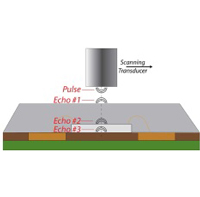
The technology uses an ultrasonic transducer that raster-scans the surface of the sample whose internal features are being imaged. While it is scanning, the transducer launches a pulse of ultrasound into the BGA package at each of millions of x-y coordinate locations, and receives the echoes from any material interfaces that the pulse encounters at those locations. The transducer carries out this function at several thousand x-y locations per second while it is scanning. The first material interface encountered by the pulse is the couplant-to-package-surface interface. This is the only interface where defects (other than flatness variations) do not occur. Internal defects occur at deeper interfaces, such as the mold compound-to-die interface, the mold compound-to-substrate interface, and the die-to-substrate interface.
The thinness of the BGA package and the acoustic velocity of the materials in the BGA package (mold compound around 3300 m/s, silicon around 8300 m/s) mean that a pulse launched by the acoustic micro imaging tool’s transducer arrives back as an echo in a few microseconds. And the lateral speed of the moving transducer is high: >1 m/s. This is why the transducer can collect echoes from several thousand x-y coordinates per second while scanning. At each coordinate it can collect echoes from various depths within the BGA package, because those echoes will arrive at the transducer at different times.
Editor's Note: This article originally appeared in the June 2015 issue of SMT Magazine.


